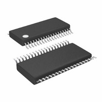
LTC3829EFE#PBF Linear Technology, LTC3829EFE#PBF Datasheet - Page 22

LTC3829EFE#PBF
Manufacturer Part Number
LTC3829EFE#PBF
Description
IC BUCK SYNC ADJ 38TSSOP
Manufacturer
Linear Technology
Type
Step-Down (Buck)r
Datasheet
1.LTC3829EFEPBF.pdf
(40 pages)
Specifications of LTC3829EFE#PBF
Internal Switch(s)
No
Synchronous Rectifier
Yes
Number Of Outputs
1
Voltage - Output
0.6 ~ 5 V
Frequency - Switching
250kHz ~ 770kHz
Voltage - Input
4.5 ~ 38 V
Operating Temperature
-40°C ~ 125°C
Mounting Type
Surface Mount
Package / Case
38-TSSOP Exposed Pad, 38-eTSSOP, 38-HTSSOP
Lead Free Status / RoHS Status
Lead free / RoHS Compliant
Current - Output
-
Power - Output
-
Available stocks
Company
Part Number
Manufacturer
Quantity
Price
LTC3829
applicaTions inForMaTion
Power MOSFET and Schottky Diode
(Optional) Selection
At least two external power MOSFETs must be selected for
each of the three output sections: One N-channel MOSFET
for the top (main) switch and one or more N-channel
MOSFET(s) for the bottom (synchronous) switch. The
number, type and on-resistance of all MOSFETs selected
take into account the voltage step-down ratio as well as
the actual position (main or synchronous) in which the
MOSFET will be used. A much smaller and much lower
input capacitance MOSFET should be used for the top
MOSFET in applications that have an output voltage that
is less than 1/3 of the input voltage. In applications where
V
less important for overall efficiency than its input capaci-
tance at operating frequencies above 300kHz. MOSFET
manufacturers have designed special purpose devices that
provide reasonably low on-resistance with significantly
reduced input capacitance for the main switch application
in switching regulators.
The peak-to-peak MOSFET gate drive levels are set by the
voltage, V
MOSFETs in most applications. Pay close attention to the
BV
logic-level MOSFETs are limited to 30V or less. Selection
criteria for the power MOSFETs include the on-resistance,
R
output current. MOSFET input capacitance is a combination
of several components but can be taken from the typical
gate charge curve included on most data sheets (Figure 9).
The curve is generated by forcing a constant input current
into the gate of a common source, current source loaded
stage and then plotting the gate voltage versus time.
IN
DS(ON)
DSS
>> V
V
GS
specification for the MOSFETs as well; many of the
, input capacitance, input voltage and maximum
OUT
C
CC
MILLER
, the top MOSFETs’ on-resistance is normally
a
Figure 9. Gate Charge Characteristic
, requiring the use of logic-level threshold
MILLER EFFECT
= (Q
Q
IN
B
– Q
A
)/V
b
DS
V
+
GS
–
V
+
–
3729 F09
V
DS
V
IN
The initial slope is the effect of the gate-to-source and
the gate-to-drain capacitance. The flat portion of the
curve is the result of the Miller multiplication effect of the
drain-to-gate capacitance as the drain drops the voltage
across the current source load. The upper sloping line is
due to the drain-to-gate accumulation capacitance and
the gate-to-source capacitance. The Miller charge (the
increase in coulombs on the horizontal axis from a to b
while the curve is flat) is specified for a given V
voltage, but can be adjusted for different V
multiplying the ratio of the application V
specified V
is to take the change in gate charge from points a and b
on a manufacturer’s data sheet and divide by the stated
V
lection criteria for determining the transition loss term in
the top MOSFET but is not directly specified on MOSFET
data sheets. C
definitions of these parameters are not included. When the
controller is operating in continuous mode the duty cycles
for the top and bottom MOSFETs are given by:
The power dissipation for the main and synchronous
MOSFETs at maximum output current are given by:
DS
Main Switch Duty Cycle
P
Synchronous Switc
P
SYNC
MAIN
voltage specified. C
=
=
( )
DS
V
V
V
V
IN
V
IN
OUT
CC
values. A way to estimate the C
IN
RSS
2 2
–
V
–
IN
V
1
V
I
OUT
and C
I
MAX
TH IL
MAX
2
N
( )
h h Duty Cycle
MILLER
I
OS
MAX
(
+
2
R
N
=
(
V
DR
are specified sometimes but
1 δ
T T H IL
+
V
V
1
OUT
)(
2
( )
is the most important se-
IN
(
)
C
1 δ R
R
MILLER
+
DS ON
=
•
(
f
)
V
DS ON
IN
)
)
DS
+
•
DS
(
–
V
to the curve
IN
MILLER
V
voltages by
)
OUT
DS
drain
term
3829f


