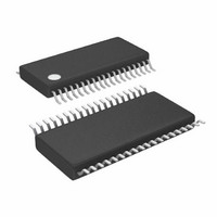
LTC3829EFE#PBF Linear Technology, LTC3829EFE#PBF Datasheet - Page 35

LTC3829EFE#PBF
Manufacturer Part Number
LTC3829EFE#PBF
Description
IC BUCK SYNC ADJ 38TSSOP
Manufacturer
Linear Technology
Type
Step-Down (Buck)r
Datasheet
1.LTC3829EFEPBF.pdf
(40 pages)
Specifications of LTC3829EFE#PBF
Internal Switch(s)
No
Synchronous Rectifier
Yes
Number Of Outputs
1
Voltage - Output
0.6 ~ 5 V
Frequency - Switching
250kHz ~ 770kHz
Voltage - Input
4.5 ~ 38 V
Operating Temperature
-40°C ~ 125°C
Mounting Type
Surface Mount
Package / Case
38-TSSOP Exposed Pad, 38-eTSSOP, 38-HTSSOP
Lead Free Status / RoHS Status
Lead free / RoHS Compliant
Current - Output
-
Power - Output
-
Available stocks
Company
Part Number
Manufacturer
Quantity
Price
applicaTions inForMaTion
1. Keep the SGND at one end of a printed circuit path thus
2. Does the IC DIFFP pin connect to the (+) plates of
3. Are the SENSE
4. Do the (+) plates of C
preventing MOSFET currents from traveling under the
IC. The INTV
immediately adjacent to the IC between the INTV
and PGND plane. A 1µF ceramic capacitor of the X7R or
X5R type is small enough to fit very close to the IC to
minimize the ill effects of the large current pulses drawn
to drive the bottom MOSFETs. An additional 5µF to 10µF
of ceramic, tantalum or other very low ESR capacitance
is recommended in order to keep the internal IC supply
quiet. The power ground returns to the sources of the
bottom N-channel MOSFETs, anodes of the Schottky
diodes and (–) plates of C
lead lengths as possible.
C
the DIFFP and V
possible to the IC.
each channel routed together with minimum PC trace
spacing? The filter capacitors between SENSE
SENSE
to the pins of the IC. Connect the SENSE
pins to the pads of the sense resistor as illustrated in
Figure 1.
topside MOSFETs as closely as possible? This capacitor
provides the pulsed current to the MOSFETs.
OUT
? A 30pF to 300pF feedforward capacitor between
–
for each channel should be as close as possible
CC
–
decoupling capacitor should be placed
FB
and SENSE
pins should be placed as close as
PWR
IN
connect to the drains of the
, which should have as short
+
printed circuit traces for
–
and SENSE
CC
+
and
pin
+
5. Keep the switching nodes, SWn, BOOSTn and TGn
6. Use a low impedance source such as a logic gate to drive
7. The 47pF to 330pF ceramic capacitor between the I
away from sensitive small-signal nodes (SENSE
SENSE
and TGn printed circuit traces should be routed away
and separated from the IC and especially the quiet side
of the IC. Separate the high dv/dt traces from sensi-
tive small-signal nodes with ground traces or ground
planes.
the PLLIN pin and keep the lead as short as possible.
pin and signal ground should be placed as close as pos-
sible to the IC. Figure 17 illustrates all branch currents
in a 3-phase switching regulator. It becomes very clear
after studying the current waveforms why it is critical to
keep the high switching current paths to a small physical
size. High electric and magnetic fields will radiate from
these loops just as radio stations transmit signals. The
output capacitor ground should return to the negative
terminal of the input capacitor and not share a common
ground path with any switched current paths. The left
half of the circuit gives rise to the noise generated by
a switching regulator. The ground terminations of the
synchronous MOSFETs and Schottky diodes should
return to the bottom plate(s) of the input capacitor(s)
with a short isolated PC trace since very high switched
currents are present. External OPTI-LOOP
tion allows overcompensation for PC layouts which are
not optimized but this is not the recommended design
procedure.
–
, DIFFP , DIFFN, V
FB
). Ideally the SWn, BOOSTn
LTC3829
®
compensa-
3829f
TH
+
,


