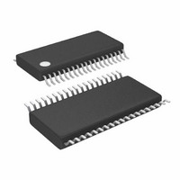
LTC3829EFE#PBF Linear Technology, LTC3829EFE#PBF Datasheet - Page 13

LTC3829EFE#PBF
Manufacturer Part Number
LTC3829EFE#PBF
Description
IC BUCK SYNC ADJ 38TSSOP
Manufacturer
Linear Technology
Type
Step-Down (Buck)r
Datasheet
1.LTC3829EFEPBF.pdf
(40 pages)
Specifications of LTC3829EFE#PBF
Internal Switch(s)
No
Synchronous Rectifier
Yes
Number Of Outputs
1
Voltage - Output
0.6 ~ 5 V
Frequency - Switching
250kHz ~ 770kHz
Voltage - Input
4.5 ~ 38 V
Operating Temperature
-40°C ~ 125°C
Mounting Type
Surface Mount
Package / Case
38-TSSOP Exposed Pad, 38-eTSSOP, 38-HTSSOP
Lead Free Status / RoHS Status
Lead free / RoHS Compliant
Current - Output
-
Power - Output
-
Available stocks
Company
Part Number
Manufacturer
Quantity
Price
operaTion
Light Load Current Operation (Burst Mode Operation,
Stage Shedding or Continuous Conduction)
The LTC3829 can be enabled to enter high efficiency
Burst Mode operation, Stage Shedding mode or forced
continuous conduction mode. To select forced continuous
operation, tie the MODE pin to a DC voltage below 0.6V
(e.g., SGND). To select Stage Shedding mode of opera-
tion, tie the MODE pin to INTV
operation, float the MODE pin.
When the controller is enabled for Burst Mode operation,
the peak current in the inductor is set to approximately
one-sixth of the maximum sense voltage even though the
voltage on the I
current can be programmed through the ISET pin. If the
average inductor current is higher than the load current,
the error amplifier, EA, will decrease the voltage on the
I
also be programmed by the ISET pin), the internal sleep
signal goes high (enabling sleep mode) and the external
MOSFETs are turned off. In sleep mode, the load current
is supplied by the output capacitor. As the output voltage
decreases, the EA’s output begins to rise. When the output
voltage drops enough, the sleep signal goes low, and the
controller resumes normal operation by turning on the top
external MOSFET on the next cycle of the internal oscillator.
When a controller is enabled for Burst Mode operation,
the inductor current is not allowed to reverse. The reverse
current comparator, I
MOSFET just before the inductor current reaches zero,
preventing it from reversing and going negative. Thus, the
controller operates in discontinuous operation. In forced
continuous operation, the inductor current is allowed to
reverse at light loads or under large transient conditions.
The peak inductor current is determined by the voltage
on the I
lower than in Burst Mode operation. However, continuous
mode has the advantages of lower output ripple and less
interference with audio circuitry.
When the MODE pin is connected to INTV
operates in Stage Shedding mode at light loads. The
controller will turn off channels 2 and 3 and increase
the current gain of the first channel to ensure smooth
TH
pin. When the I
TH
pin. In this mode, the efficiency at light loads is
TH
pin indicates a lower value. The peak
TH
(Refer to Functional Diagram)
REV
voltage drops below 0.5V (can
, turns off the bottom external
CC
. To select Burst Mode
CC
, the LTC3829
transition. The threshold where the controller goes into
Stage Shedding mode is when the I
below 0.5V, but it can be programmed by ISET pin. The
inductor current is not allowed to reverse in this mode
(discontinuous operation). At very light loads, the current
comparator may remain tripped for several cycles and
force the external top MOSFET to stay off for the same
number of cycles (i.e., skipping pulses). This mode ex-
hibits low output ripple as well as low audio noise and
reduced RF interference as compared to Burst Mode
operation. It provides higher low current efficiency than
forced continuous mode, but not nearly as high as Burst
Mode operation.
2-Chip Operations (CLKOUT Pin)
The LTC3829’s three channels are 120° out of phase
providing multiphase operation. This configuration can
provide enough power for most high current applications.
However, for even higher power applications, the LTC3829
can be configured for PolyPhase
The LTC3829 features a CLKOUT pin which enables two
LTC3829s to operate out of phase. The CLKOUT signal is
60° out of phase with respect to phase 1 of the controller. In
Stage Shedding mode, however, the CLKOUT signal is 180°
out of phase with respect to phase 1 of the controller.
Frequency Selection and Phase-Locked Loop
(FREQ and PLLIN Pins)
The selection of switching frequency is a trade-off between
efficiency and component size. Low frequency opera-
tion increases efficiency by reducing MOSFET switching
losses, but requires larger inductance and/or capacitance
to maintain low output ripple voltage.
If the PLLIN pin is not being driven by an external clock
source, the FREQ pin can be used to program the controller’s
operating frequency from 250kHz to 770kHz. There is a
precision 10µA current flowing out of the FREQ pin so that
the user can program the controller’s switching frequency
with a single resistor to SGND. A curve is provided later in
the Applications Information section showing the relation-
ship between the voltage on the FREQ pin and switching
frequency.
®
and 2-chip operation.
TH
LTC3829
voltage drops
3829f


