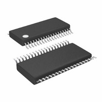
LTC3829EFE#PBF Linear Technology, LTC3829EFE#PBF Datasheet - Page 33

LTC3829EFE#PBF
Manufacturer Part Number
LTC3829EFE#PBF
Description
IC BUCK SYNC ADJ 38TSSOP
Manufacturer
Linear Technology
Type
Step-Down (Buck)r
Datasheet
1.LTC3829EFEPBF.pdf
(40 pages)
Specifications of LTC3829EFE#PBF
Internal Switch(s)
No
Synchronous Rectifier
Yes
Number Of Outputs
1
Voltage - Output
0.6 ~ 5 V
Frequency - Switching
250kHz ~ 770kHz
Voltage - Input
4.5 ~ 38 V
Operating Temperature
-40°C ~ 125°C
Mounting Type
Surface Mount
Package / Case
38-TSSOP Exposed Pad, 38-eTSSOP, 38-HTSSOP
Lead Free Status / RoHS Status
Lead free / RoHS Compliant
Current - Output
-
Power - Output
-
Available stocks
Company
Part Number
Manufacturer
Quantity
Price
applicaTions inForMaTion
Efficiency Considerations
The percent efficiency of a switching regulator is equal to
the output power divided by the input power times 100%.
It is often useful to analyze individual losses to determine
what is limiting the efficiency and which change would
produce the most improvement. Percent efficiency can
be expressed as:
where L1, L2, etc. are the individual losses as a percent-
age of input power.
Although all dissipative elements in the circuit produce
losses, four main sources usually account for most of the
losses in LTC3829 circuits: 1) IC V
regulator current, 3) I
transition losses.
1. The V
2. INTV
%Efficiency = 100% – (L1 + L2 + L3 + ...)
Electrical Characteristics table, which excludes MOSFET
driver and control currents. V
in a small (<0.1%) loss.
control currents. The MOSFET driver current results
from switching the gate capacitance of the power
MOSFETs. Each time a MOSFET gate is switched from
low to high to low again, a packet of charge dQ moves
from INTV
out of INTV
control circuit current. In continuous mode, I
f(Q
topside and bottom side MOSFETs. Supplying INTV
power through EXTV
will scale the V
control circuits by a factor of (duty cycle)/(efficiency).
For example, in a 20V to 5V application, 10mA of
INTV
current. This reduces the mid-current loss from 10%
or more (if the driver was powered directly from V
to only a few percent.
T
+ Q
CC
CC
IN
current results in approximately 2.5mA of V
current is the sum of the MOSFET driver and
B
current is the DC supply current given in the
), where Q
CC
CC
to ground. The resulting dQ/dt is a current
that is typically much larger than the
IN
current required for the driver and
T
and Q
CC
2
R losses, 4) topside MOSFET
from an output-derived source
B
are the gate charges of the
IN
current typically results
IN
current, 2) INTV
GATECHG
IN
CC
CC
IN
=
)
3. I
4. Transition losses apply only to the topside MOSFET(s),
the fuse (if used), MOSFET, inductor and current sense
resistor. In continuous mode, the average output current
flows through L and R
the topside MOSFET and the synchronous MOSFET. If
the two MOSFETs have approximately the same R
then the resistance of one MOSFET can simply be
summed with the resistances of L and R
tain I
R
25mΩ. This results in losses ranging from 2% to 8%
as the output current increases from 3A to 15A for a 5V
output, or a 3% to 12% loss for a 3.3V output.
Efficiency varies as the inverse square of V
same external components and output power level. The
combined effects of increasingly lower output voltages
and higher currents required by high performance digital
systems is not doubling but quadrupling the importance
of loss terms in the switching regulator system!
and become significant only when operating at high
input voltages (typically 15V or greater). Transition
losses can be estimated from:
Other hidden losses such as copper trace and internal
battery resistances can account for an additional 5%
to 10% efficiency degradation in portable systems. It
is very important to include these system level losses
during the design phase. The internal battery and fuse
resistance losses can be minimized by making sure that
C
the switching frequency. A 25W supply will typically
require a minimum of 20µF to 40µF of capacitance
having a maximum of 20mΩ to 50mΩ of ESR. Other
losses including Schottky conduction losses during
dead time and inductor core losses generally account
for less than 2% total additional loss.
2
IN
L
R losses are predicted from the DC resistances of
Transition Loss = (1.7) V
= 10mΩ, R
has adequate charge storage and very low ESR at
2
R losses. For example, if each R
SENSE
= 5mΩ, then the total resistance is
SENSE
IN
, but is chopped between
2
• I
O(MAX)
LTC3829
DS(ON)
• C
SENSE
OUT
RSS
= 10mΩ,
DS(ON)
for the
• f
to ob-
3829f
,


