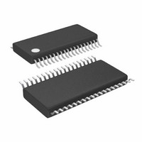
LTC3829EFE#PBF Linear Technology, LTC3829EFE#PBF Datasheet - Page 14

LTC3829EFE#PBF
Manufacturer Part Number
LTC3829EFE#PBF
Description
IC BUCK SYNC ADJ 38TSSOP
Manufacturer
Linear Technology
Type
Step-Down (Buck)r
Datasheet
1.LTC3829EFEPBF.pdf
(40 pages)
Specifications of LTC3829EFE#PBF
Internal Switch(s)
No
Synchronous Rectifier
Yes
Number Of Outputs
1
Voltage - Output
0.6 ~ 5 V
Frequency - Switching
250kHz ~ 770kHz
Voltage - Input
4.5 ~ 38 V
Operating Temperature
-40°C ~ 125°C
Mounting Type
Surface Mount
Package / Case
38-TSSOP Exposed Pad, 38-eTSSOP, 38-HTSSOP
Lead Free Status / RoHS Status
Lead free / RoHS Compliant
Current - Output
-
Power - Output
-
Available stocks
Company
Part Number
Manufacturer
Quantity
Price
LTC3829
operaTion
A phase-locked loop (PLL) is available on the LTC3829
to synchronize the internal oscillator to an external clock
source that is connected to the PLLIN pin. The PLL loop
filter network is integrated inside the LTC3829. The phase-
locked loop is capable of locking any frequency within
the range of 250kHz to 770kHz. The frequency setting
resistor should always be present to set the controller’s
initial switching frequency before locking to the external
clock. The controller is operating in forced continuous
mode when it is synchronized.
Sensing the Output Voltage with a
Differential Amplifier
The LTC3829 includes a low offset, unity-gain, high band-
width differential amplifier for applications that require true
remote sensing. Sensing the load across the load capaci-
tors directly greatly benefits regulation in high current, low
voltage applications, where board interconnection losses
can be a significant portion of the total error budget.
The LTC3829 differential amplifier has a typical output slew
rate of 2V/µs. The amplifier is configured for unity gain,
meaning that the difference between DIFFP and DIFFN is
translated to DIFFOUT, relative to SGND.
Care should be taken to route the DIFFP and DIFFN PCB
traces parallel to each other all the way to the terminals
of the output capacitor or remote sensing points on the
board. In addition, avoid routing these sensitive traces
near any high speed switching nodes in the circuit. Ideally,
the DIFFP and DIFFN traces should be shielded by a low
impedance ground plane to maintain signal integrity.
The maximum output voltage when using the differential
amplifier is INTV
voltage the differential amplifier should not be used.
Power Good (PGOOD Pin)
The PGOOD pin is connected to an open drain of an
internal N-channel MOSFET. The MOSFET turns on and
pulls the PGOOD pin low when the V
CC
– 1.4V (typically 3.6V). Above this output
(Refer to Functional Diagram)
FB
pin voltage is not
within ±10% of the 0.6V reference voltage. The PGOOD
pin is also pulled low when the RUN pin is below 1.22V or
when the LTC3829 is in the soft-start or tracking phase.
When the V
window, the MOSFET is turned off and the pin is allowed
to be pulled up by an external resistor to a source of up
to 6V. The PGOOD pin will flag power good immediately
when the V
there is an internal 100µs power-bad mask when the V
goes out of the window.
Output Overvoltage Protection
An overvoltage comparator, OV, guards against transient
overshoots (>10%) as well as other more serious condi-
tions that may overvoltage the output. In such cases, the
top MOSFET is turned off and the bottom MOSFET is turned
on until the overvoltage condition is cleared.
Undervoltage Lockout
The LTC3829 has two functions that help protect the
controller in case of undervoltage conditions. A precision
UVLO comparator constantly monitors the INTV
to ensure that an adequate gate-drive voltage is present. It
locks out the switching action when INTV
To prevent oscillation when there is a disturbance on the
INTV
hysteresis.
Another way to detect an undervoltage condition is to moni-
tor the V
turn-on reference of 1.22V, one can use a resistor divider
to V
4.5µA of current flows out of the RUN pin once the RUN
pin voltage passes 1.22V. The RUN comparator itself has
about 80mV of hysteresis. One can program additional
hysteresis for the RUN comparator by adjusting the val-
ues of the resistive divider. For accurate V
detection, V
IN
CC
to turn on the IC when V
, the UVLO comparator has 600mV of precision
IN
FB
supply. Because the RUN pin has a precision
FB
IN
pin is within the regulation window. However,
needs to be higher than 4.5V.
pin voltage is within the ±10% regulation
IN
is high enough. An extra
CC
IN
is below 3.3V.
undervoltage
CC
voltage
3829f
FB


