LTC3829EFE#PBF Linear Technology, LTC3829EFE#PBF Datasheet - Page 9
LTC3829EFE#PBF
Manufacturer Part Number
LTC3829EFE#PBF
Description
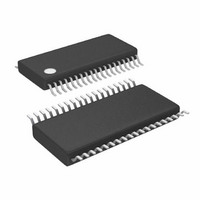
IC BUCK SYNC ADJ 38TSSOP
Manufacturer
Linear Technology
Type
Step-Down (Buck)r
Datasheet
1.LTC3829EFEPBF.pdf
(40 pages)
Specifications of LTC3829EFE#PBF
Internal Switch(s)
No
Synchronous Rectifier
Yes
Number Of Outputs
1
Voltage - Output
0.6 ~ 5 V
Frequency - Switching
250kHz ~ 770kHz
Voltage - Input
4.5 ~ 38 V
Operating Temperature
-40°C ~ 125°C
Mounting Type
Surface Mount
Package / Case
38-TSSOP Exposed Pad, 38-eTSSOP, 38-HTSSOP
Lead Free Status / RoHS Status
Lead free / RoHS Compliant
Current - Output
-
Power - Output
-
Available stocks
Company
Part Number
Manufacturer
Quantity
Price


pin FuncTions
DIFFN (Pin 1/Pin 3): Negative Input of Remote Sensing
Differential Amplifier. Connect this to the remote load
ground pin.
DIFFP (Pin 2/Pin 4): Positive Input of Remote Sensing
Differential Amplifier. Connect this to the remote load
positive terminal directly.
RUN (Pin 3/Pin 5): Run Control Input. A voltage above
1.22V on this pin turns on the IC. There is a 1.0µA pull-up
current for this pin. Once the RUN pin rises above 1.22V,
an additional 4.5µA pull-up current is added to the pin.
AVP (Pin 4/Pin 6): Active Voltage Positioning Load Slope
Programming Pin. A resistor tied between this pin and the
DIFFP pin sets the load slope.
SENSE1
13): Current Sense Comparator Inputs. The (+) inputs to
the current comparators are normally connected to DCR
sensing networks or current sensing resistors.
SENSE1
14): Current Sense Comparator Inputs. The (–) inputs to
the current comparators are connected to the output.
TK/SS (Pin 9/Pin 11): Output Voltage Tracking and Soft-
Start Input. When one particular IC is configured to be the
master of two ICs, a capacitor to ground at this pin sets
the ramp rate for the master IC’s output voltage. When the
IC is configured to be the slave of two ICs, the V
of the master IC is reproduced by a resistor divider and
applied to this pin. An internal soft-start current of 1.25µA
is charging this pin.
FREQ (Pin 10/Pin 12): There is a precision 10µA current
sourced out of this pin. A resistor to ground sets a voltage
which in turn programs the frequency. Alternatively, this
pin can be driven with a DC voltage to vary the frequency
of the internal oscillator.
V
pin receives the remotely sensed feedback voltage from
an external resistive divider.
I
Amplifier Compensation Point. Each associated channels’
current comparator tripping threshold increases with this
I
TH
TH
FB
(Pin 14/Pin 16): Current Control Threshold and Error
control voltage.
(Pin 13/Pin 15): Error Amplifier Feedback Input. This
+
–
, SENSE2
, SENSE2
–
+
, SENSE3
, SENSE3
(UHF/FE)
–
+
(Pins 6, 8, 12/Pins 8, 10,
(Pins 5, 7, 11/Pins 7, 9,
FB
voltage
ISET (Pin 15/Pin 17): Stage Shedding Comparator and
Burst Mode Comparator Programming Pin. A resistor to
ground programs the stage shedding comparator threshold
or Burst Mode comparator threshold and its current limit
depending on MODE pin setting.
I
Range Pin. This pin is to be programmed to SGND, FLOAT
or INTV
one of three different levels for each comparator.
PGOOD (Pin 17/Pin 19): Power Good Indicator Output.
Open-drain logic out that is pulled to ground when the
output exceeds ±10% regulation window after the internal
100µs power bad mask timer expires.
PLLIN (Pin 18/Pin 20): External Synchronization Pin. A
clock on the pin synchronizes the internal oscillator with
the clock on this pin.
EXTV
Internal Switch Connected to INTV
and supplies the IC power, bypassing the internal low
dropout regulator, whenever EXTV
Do not exceed 6V on this pin and ensure V
at all times.
INTV
control circuits are powered from this voltage. Decouple
this pin to PGND with a minimum of 4.7µF low ESR tan-
talum or ceramic capacitor.
V
to PGND with a capacitor (0.1µF to 1µF).
BG1, BG2, BG3 (Pins 30, 29, 22/Pins 32, 31, 24): Bottom
Gate Driver Outputs. These pins drive the gates of the bot-
tom N-channel MOSFETs between PGND and INTV
SW1, SW2, SW3 (Pins 31, 28, 21/Pins 33, 30, 23):
Switch Node Connections to Inductors. Voltage swing
at these pins is from a Schottky diode (external) voltage
drop below ground to V
TG1, TG2, TG3 (Pins 32, 27, 20/Pins 34, 29, 22): Top Gate
Driver Outputs. These are the outputs of floating drivers
with a voltage swing equal to INTV
the switch nodes voltages.
LIM
IN
(Pin 25/Pin 27): Main Input Supply. Decouple this pin
(Pin 16/Pin 18): Current Comparator Sense Voltage
CC
CC
CC
(Pin 24/Pin 26): Internal 5V Regulator Output. The
(Pin 23/Pin 25): External Power Input to an
to set the maximum current sense threshold to
IN
.
CC
CC
CC
. This switch closes
is higher than 4.7V.
superimposed on
LTC3829
IN
> V
EXTVCC
CC
.
3829f
Related parts for LTC3829EFE#PBF
Image
Part Number
Description
Manufacturer
Datasheet
Request
R

Part Number:
Description:
CD ROM LINEARVIEW DATASHEETS
Manufacturer:
Linear Technology

Part Number:
Description:
Standalone Linear Li-Ion Battery Charger with Thermal Regulation in ThinSOT
Manufacturer:
Linear Technology Corporation
Datasheet:
Part Number:
Description:
Low noise, high frequency, 8th order linear phase lowpass filter
Manufacturer:
Linear Technology Corporation
Datasheet:
Part Number:
Description:
Manufacturer:
Linear Technology Corporation
Datasheet:
Part Number:
Description:
Manufacturer:
Linear Technology Corporation
Datasheet:
Part Number:
Description:
Manufacturer:
Linear Technology Corporation
Datasheet:
Part Number:
Description:
Manufacturer:
Linear Technology Corporation
Datasheet:
Part Number:
Description:
Manufacturer:
Linear Technology Corporation
Datasheet:
Part Number:
Description:
Manufacturer:
Linear Technology Corporation
Datasheet:
Part Number:
Description:
Manufacturer:
Linear Technology Corporation
Datasheet:
Part Number:
Description:
Dual and Quad, JFET Input Precision High Speed Op Amps
Manufacturer:
Linear Technology Corporation
Datasheet:
Part Number:
Description:
Manufacturer:
Linear Technology Corporation
Datasheet:
Part Number:
Description:
1, 2, 6 and 8 Channel, 10-Bit Serial I/O Data Acquisition Systems
Manufacturer:
Linear Technology Corporation
Datasheet:
Part Number:
Description:
Manufacturer:
Linear Technology Corporation
Datasheet:
Part Number:
Description:
Universal dual filter building block
Manufacturer:
Linear Technology Corporation
Datasheet: