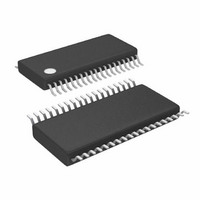
LTC3829EFE#PBF Linear Technology, LTC3829EFE#PBF Datasheet - Page 34

LTC3829EFE#PBF
Manufacturer Part Number
LTC3829EFE#PBF
Description
IC BUCK SYNC ADJ 38TSSOP
Manufacturer
Linear Technology
Type
Step-Down (Buck)r
Datasheet
1.LTC3829EFEPBF.pdf
(40 pages)
Specifications of LTC3829EFE#PBF
Internal Switch(s)
No
Synchronous Rectifier
Yes
Number Of Outputs
1
Voltage - Output
0.6 ~ 5 V
Frequency - Switching
250kHz ~ 770kHz
Voltage - Input
4.5 ~ 38 V
Operating Temperature
-40°C ~ 125°C
Mounting Type
Surface Mount
Package / Case
38-TSSOP Exposed Pad, 38-eTSSOP, 38-HTSSOP
Lead Free Status / RoHS Status
Lead free / RoHS Compliant
Current - Output
-
Power - Output
-
Available stocks
Company
Part Number
Manufacturer
Quantity
Price
LTC3829
applicaTions inForMaTion
Checking Transient Response
The regulator loop response can be checked by looking at
the load current transient response. Switching regulators
take several cycles to respond to a step in DC (resistive)
load current. When a load step occurs, V
amount equal to ∆I
series resistance of C
discharge C
forces the regulator to adapt to the current change and
return V
time V
ringing, which would indicate a stability problem. The
availability of the I
control loop behavior but also provides a DC-coupled and
AC-filtered closed-loop response test point. The DC step,
rise time and settling at this test point truly reflects the
closed-loop response. Assuming a predominantly second
order system, phase margin and/or damping factor can be
estimated using the percentage of overshoot seen at this
pin. The bandwidth can also be estimated by examining the
rise time at the pin. The I
in the Typical Application circuit will provide an adequate
starting point for most applications. The I
filter sets the dominant pole-zero loop compensation.
The values can be modified slightly (from 0.5 to 2 times
their suggested values) to optimize transient response
once the final PC layout is done and the particular output
capacitor type and value have been determined. The output
capacitors need to be selected because the various types
and values determine the loop gain and phase. An output
current pulse of 20% to 80% of full-load current having
a rise time of 1µs to 10µs will produce output voltage and
I
stability without breaking the feedback loop. Placing a
power MOSFET directly across the output capacitor and
TH
pin waveforms that will give a sense of the overall loop
OUT
OUT
can be monitored for excessive overshoot or
OUT
to its steady-state value. During this recovery
generating the feedback error signal that
TH
LOAD (ESR)
OUT
pin not only allows optimization of
. ∆I
TH
LOAD
external components shown
, where ESR is the effective
also begins to charge or
OUT
TH
series R
shifts by an
C
-C
C
driving the gate with an appropriate signal generator is a
practical way to produce a realistic load step condition. The
initial output voltage step resulting from the step change
in output current may not be within the bandwidth of the
feedback loop, so this signal cannot be used to determine
phase margin. This is why it is better to look at the I
pin signal which is in the feedback loop and is the filtered
and compensated control loop response. The gain of the
loop will be increased by increasing R
of the loop will be increased by decreasing C
increased by the same factor that C
zero frequency will be kept the same, thereby keeping the
phase shift the same in the most critical frequency range
of the feedback loop. The output voltage settling behavior
is related to the stability of the closed-loop system and
will demonstrate the actual overall supply performance.
A second, more severe transient is caused by switching
in loads with large (>1µF) supply bypass capacitors. The
discharged bypass capacitors are effectively put in parallel
with C
alter its delivery of current quickly enough to prevent this
sudden step change in output voltage if the load switch
resistance is low and it is driven quickly. If the ratio of
C
should be controlled so that the load rise time is limited
to approximately 25 • C
require a 250µs rise time, limiting the charging current
to about 200mA.
PC Board Layout Checklist
When laying out the printed circuit board, the following
checklist should be used to ensure proper operation of
the IC. These items are also illustrated graphically in the
layout diagram of Figure 17. Check the following in the
PC layout:
LOAD
OUT
to C
, causing a rapid drop in V
OUT
is greater than 1:50, the switch rise time
LOAD
. Thus a 10µF capacitor would
OUT
C
C
and the bandwidth
is decreased, the
. No regulator can
C
. If R
C
3829f
TH
is


