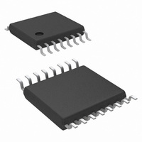
LM25088MH-1/NOPB National Semiconductor, LM25088MH-1/NOPB Datasheet - Page 11

LM25088MH-1/NOPB
Manufacturer Part Number
LM25088MH-1/NOPB
Description
IC CTLR BUCK NON-SYNC 16-TSSOP
Manufacturer
National Semiconductor
Series
PowerWise®r
Type
Step-Down (Buck)r
Datasheet
1.LM25088MH-2NOPB.pdf
(28 pages)
Specifications of LM25088MH-1/NOPB
Design Resources
LM(2)5088-1/2 QS Component Calculator
Internal Switch(s)
No
Synchronous Rectifier
No
Number Of Outputs
1
Voltage - Output
1.21 ~ 45 V
Current - Output
10A
Frequency - Switching
200kHz, 500kHz
Voltage - Input
4.5 ~ 42 V
Operating Temperature
-40°C ~ 125°C
Mounting Type
Surface Mount
Package / Case
16-TSSOP Exposed Pad, 16-eTSSOP, 16-HTSSOP
Primary Input Voltage
42V
No. Of Outputs
1
Output Voltage
1.2V
Output Current
10A
No. Of Pins
16
Operating Temperature Range
-40°C To +125°C
Msl
MSL 1 - Unlimited
Filter Terminals
SMD
Rohs Compliant
Yes
Lead Free Status / RoHS Status
Lead free / RoHS Compliant
Power - Output
-
Other names
LM25088MH-1
Available stocks
Company
Part Number
Manufacturer
Quantity
Price
Company:
Part Number:
LM25088MH-1/NOPB
Manufacturer:
NSC
Quantity:
800
Error Amplifier and PWM
Comparator
The internal high gain error amplifier generates an error signal
proportional to the difference between the regulated output
voltage and an internal precision voltage reference (1.205V).
The output of the error amplifier is connected to the COMP
pin allowing the user to connect loop compensation compo-
nents. Generally a type II network, as illustrated in Figure 1,
is sufficient. This network creates a pole at DC, a mid-band
zero for phase boost and a high frequency pole for noise re-
duction. The PWM comparator compares the emulated cur-
rent signal from the RAMP generator to the error amplifier
output voltage at the COMP pin. A typical control loop gain/
phase plot is shown in performance curves section of this
document.
FIGURE 2. Basic Enable Configuration
11
Ramp Generator
The ramp signal used for the pulse width modulator in current
mode control is typically derived directly from the buck switch
current. This signal corresponds to the positive slope portion
of the buck inductor current. Using this signal for the PWM
ramp simplifies the control loop transfer function to a single
pole response and provides inherent input voltage feed-for-
ward compensation. The disadvantage of using the buck
switch current signal for PWM control is the large leading
edge spike due to circuit parasitics which must be filtered or
blanked. Also, the current measurement may introduce sig-
nificant propagation delays. The filtering time, blanking time
and propagation delay limit the minimum achievable pulse
width. In applications where the input voltage may be rela-
tively large in comparison to the output voltage, controlling
small pulse widths and duty cycles is necessary for regulation.
The LM25088 utilizes a unique ramp generator which does
not actually measure the buck switch current but rather re-
constructs or emulates the signal. Emulating the inductor
current provides a ramp signal that is free of leading edge
spikes and measurement or filtering delays. The current re-
construction is comprised of two elements; a sample & hold
DC level and an emulated current ramp.
30087605
www.national.com


