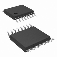
LM25088MH-1/NOPB National Semiconductor, LM25088MH-1/NOPB Datasheet - Page 12

LM25088MH-1/NOPB
Manufacturer Part Number
LM25088MH-1/NOPB
Description
IC CTLR BUCK NON-SYNC 16-TSSOP
Manufacturer
National Semiconductor
Series
PowerWise®r
Type
Step-Down (Buck)r
Datasheet
1.LM25088MH-2NOPB.pdf
(28 pages)
Specifications of LM25088MH-1/NOPB
Design Resources
LM(2)5088-1/2 QS Component Calculator
Internal Switch(s)
No
Synchronous Rectifier
No
Number Of Outputs
1
Voltage - Output
1.21 ~ 45 V
Current - Output
10A
Frequency - Switching
200kHz, 500kHz
Voltage - Input
4.5 ~ 42 V
Operating Temperature
-40°C ~ 125°C
Mounting Type
Surface Mount
Package / Case
16-TSSOP Exposed Pad, 16-eTSSOP, 16-HTSSOP
Primary Input Voltage
42V
No. Of Outputs
1
Output Voltage
1.2V
Output Current
10A
No. Of Pins
16
Operating Temperature Range
-40°C To +125°C
Msl
MSL 1 - Unlimited
Filter Terminals
SMD
Rohs Compliant
Yes
Lead Free Status / RoHS Status
Lead free / RoHS Compliant
Power - Output
-
Other names
LM25088MH-1
Available stocks
Company
Part Number
Manufacturer
Quantity
Price
Company:
Part Number:
LM25088MH-1/NOPB
Manufacturer:
NSC
Quantity:
800
www.national.com
The sample & hold DC level illustrated in Figure 3 is derived
from a measurement of the re-circulating (or free-wheeling)
diode current. The diode current flows through the current
sense resistor connected between the CS and CSG pins. The
voltage across the sense resistor is sampled and held just
prior to the onset of the next conduction interval of the buck
switch. The diode current sensing and sample & hold provide
the DC level for the reconstructed current signal. The positive
slope inductor current ramp is emulated by an external ca-
pacitor connected from the RAMP pin to GND and an internal
voltage controlled current source. The ramp current source
that emulates the inductor current is a function of the VIN and
VOUT voltages per the following equation:
Proper selection of the RAMP capacitor depends upon the
selected value of the output inductor and the current sense
resistor (R
hold value and the ramp amplitude must have the same de-
pendence on the load current. That is:
Where, g
µA/V) and A is the gain of the current sense amplifier (10V/
V). The RAMP capacitor should connected directly to the
RAMP and GND pins of the IC.
For duty cycles greater than 50%, peak current mode control
circuits are subject to sub-harmonic oscillation. Sub-harmonic
m
I
S
RAMP
is the ramp current generator transconductance (5
). For proper current emulation, the DC sample &
= 5 µA/V x (VIN x VOUT) + 25 µA
FIGURE 3. Composition of Current Sense Signal
12
oscillation is normally characterized by alternating wide and
narrow pulses at the SW pin. Adding a fixed slope voltage
ramp (slope compensation) to the current sense signal pre-
vents this oscillation. The 25 µA offset current supplied by the
emulated current source provides a fixed slope to the ramp
signal. In some high output voltage, high duty cycles applica-
tions; additional slope compensation may be required. In
these applications, a pull-up resistor may be added between
the RAMP and VCC pins to increase the ramp slope com-
pensation. A formula to configure pull-up resistor is shown in
Applications Information section.
Dropout Voltage Reduction
The LM25088 features unique circuitry to reduce the dropout
voltage. Dropout voltage is defined as the difference between
the minimum input voltage to maintain regulation and the out-
put voltage (VIN
the lowest input voltage at which the converter maintains reg-
ulation. In a buck converter, dropout voltage primarily de-
pends upon the maximum duty cycle. The maximum duty
cycle is dependant on the oscillator frequency and minimum
off-time.
An approximation for the dropout voltage is:
min
- Vout). Dropout voltage thus determines
30087607


