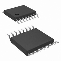
LM25088MH-1/NOPB National Semiconductor, LM25088MH-1/NOPB Datasheet - Page 18

LM25088MH-1/NOPB
Manufacturer Part Number
LM25088MH-1/NOPB
Description
IC CTLR BUCK NON-SYNC 16-TSSOP
Manufacturer
National Semiconductor
Series
PowerWise®r
Type
Step-Down (Buck)r
Datasheet
1.LM25088MH-2NOPB.pdf
(28 pages)
Specifications of LM25088MH-1/NOPB
Design Resources
LM(2)5088-1/2 QS Component Calculator
Internal Switch(s)
No
Synchronous Rectifier
No
Number Of Outputs
1
Voltage - Output
1.21 ~ 45 V
Current - Output
10A
Frequency - Switching
200kHz, 500kHz
Voltage - Input
4.5 ~ 42 V
Operating Temperature
-40°C ~ 125°C
Mounting Type
Surface Mount
Package / Case
16-TSSOP Exposed Pad, 16-eTSSOP, 16-HTSSOP
Primary Input Voltage
42V
No. Of Outputs
1
Output Voltage
1.2V
Output Current
10A
No. Of Pins
16
Operating Temperature Range
-40°C To +125°C
Msl
MSL 1 - Unlimited
Filter Terminals
SMD
Rohs Compliant
Yes
Lead Free Status / RoHS Status
Lead free / RoHS Compliant
Power - Output
-
Other names
LM25088MH-1
Available stocks
Company
Part Number
Manufacturer
Quantity
Price
Company:
Part Number:
LM25088MH-1/NOPB
Manufacturer:
NSC
Quantity:
800
www.national.com
OUTPUT CAPACITORS
The output capacitors smooth the inductor current ripple and
provide a source of charge for load transient conditions. The
output capacitor selection is primarily dictated by the following
specifications:
1. Steady-state output peak-peak ripple (ΔV
2. Output voltage deviation during transient condition (ΔV
sient
For the 5V output design example, ΔV
VOUT) and ΔT
The magnitude of output ripple primarily depends on ESR of
the capacitors while load transient voltage deviation depends
both on the output capacitance and ESR.
When a full load is suddenly removed from the output, the
output capacitor must be large enough to prevent the inductor
energy to raise the output voltage above the specified maxi-
mum voltage. In other words, the output capacitor must be
large enough to absorb the inductor’s maximum stored ener-
gy. Equating, the stored energy equations of both the inductor
and the output capacitor it can be shown that:
Evaluating, the above equation with a ΔVout of 100 mV re-
sults in an output capacitance of 475 µF. As stated earlier, the
maximum peak to peak ripple primarily depends on the ESR
of the output capacitor and the inductor ripple current. To sat-
isfy the ΔV
ESR should be less than 15 mΩ. In this design example a 470
µF aluminum capacitor with an ESR of 10 mΩ is paralleled
with two 47 µF ceramic capacitors to further reduce the ESR.
INPUT CAPACITORS
The input power supply typically has large source impedance
at the switching frequency. Good quality input capacitors are
necessary to limit the ripple voltage at the VIN pin while sup-
plying most of the switch current during the on-time. When the
buck switch turns ON, the current into the external FET steps
to the valley of the inductor current waveform at turn-on,
ramps up to the peak value, and then drops to zero at turn-
)
FIGURE 10. Additional Slope Compensation for
PK-PK
Transient
of 50 mV with 40% inductor current ripple, the
= 100 mV (2% of VOUT) was chosen.
VOUT > 5V
30087626
PK-PK
PK-PK
= 50 mV (1% of
)
Tran-
18
off. The input capacitors should be selected for RMS current
rating and minimum ripple voltage. A good approximation for
the ripple current is I
Quality ceramic capacitors with a low ESR should be selected
for the input filter. To allow for capacitor tolerances and volt-
age rating, five 2.2 µF, 100V ceramic capacitors were select-
ed. With ceramic capacitors, the input ripple voltage will be
triangular and will peak at 50% duty cycle. Taking into account
the capacitance change with DC bias a worst case input peak-
to-peak ripple voltage can be approximated as:
When the converter is connected to an input power source, a
resonant circuit is formed by the line impedance and the input
capacitors. This can result in an overshoot at the VIN pin and
could result in VIN exceeding its absolute maximum rating.
Because of those conditions, it is recommended that either
an aluminum type capacitor with an ESR or increasing
CIN>10 x LIN While using aluminum type capacitor care
should be taken to not exceed its maximum ripple current rat-
ing. Tantalum capacitors must be avoided at the input as they
are prone to shorting.
VCC CAPACITOR
The capacitor at the VCC pin provides noise filtering and sta-
bility for the VCC regulator. The recommended value should
be no smaller than 0.1 µF, and should be a good quality, low
ESR, ceramic capacitor. A value of 1 µF was selected for this
design.
BOOTSTRAP CAPACITOR
The bootstrap capacitor between HB and SW pins supplies
the gate current to charge the high-side MOSFET gate at
each cycle’s turn-on as well as supplying the recovery charge
for the bootstrap diode (D1).The peak current can be several
amperes. The recommended value of the bootstrap capacitor
is at least 0.022 µF and should be a good quality, low ESR,
ceramic capacitor located close to the pins of the IC. The ab-
solute minimum value for the bootstrap capacitor is calculated
as:
Where, Q
is the tolerable voltage droop on C
than 5% of the VCC. A value of 0.1 µF was selected for this
design.
SOFT-START CAPACITOR
The capacitor at the SS capacitor determines the soft-start
time, the output voltage to reach the final regulated value. The
value of C
For this design example, a value of 0.022 µF was chosen for
a soft start time of approximately 2 ms.
g
SS
is the high-side MOSFET gate charge and ΔV
for a given time is determined from:
RMS
> I
OUT
/2.
HB
, which is typically less
HB


