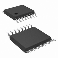
LM25088MH-1/NOPB National Semiconductor, LM25088MH-1/NOPB Datasheet - Page 20

LM25088MH-1/NOPB
Manufacturer Part Number
LM25088MH-1/NOPB
Description
IC CTLR BUCK NON-SYNC 16-TSSOP
Manufacturer
National Semiconductor
Series
PowerWise®r
Type
Step-Down (Buck)r
Datasheet
1.LM25088MH-2NOPB.pdf
(28 pages)
Specifications of LM25088MH-1/NOPB
Design Resources
LM(2)5088-1/2 QS Component Calculator
Internal Switch(s)
No
Synchronous Rectifier
No
Number Of Outputs
1
Voltage - Output
1.21 ~ 45 V
Current - Output
10A
Frequency - Switching
200kHz, 500kHz
Voltage - Input
4.5 ~ 42 V
Operating Temperature
-40°C ~ 125°C
Mounting Type
Surface Mount
Package / Case
16-TSSOP Exposed Pad, 16-eTSSOP, 16-HTSSOP
Primary Input Voltage
42V
No. Of Outputs
1
Output Voltage
1.2V
Output Current
10A
No. Of Pins
16
Operating Temperature Range
-40°C To +125°C
Msl
MSL 1 - Unlimited
Filter Terminals
SMD
Rohs Compliant
Yes
Lead Free Status / RoHS Status
Lead free / RoHS Compliant
Power - Output
-
Other names
LM25088MH-1
Available stocks
Company
Part Number
Manufacturer
Quantity
Price
Company:
Part Number:
LM25088MH-1/NOPB
Manufacturer:
NSC
Quantity:
800
www.national.com
ERROR AMPLIFIER COMPENSATION
R
characteristics to accomplish a stable voltage loop gain. One
advantage of current mode control is the ability of to close the
loop with only two feedback components R
The voltage loop gain is the product of the modulator gain and
the error amplifier gain. For this example, the modulator can
be treated as an ideal voltage-to-current (transconductance)
converter, The DC modulator gain of the LM25088 can be
modeled as:
DC Gain
The dominant low frequency pole of the modulator is deter-
mined by the load resistance (R
tance (C
For, R
then FP
DC Gain
For the 5V design example the modulator gain vs. frequency
characteristic was measured as shown in Figure 11.
Components R
as a type II compensation configuration. The DC gain of the
amplifier is 80dB which has a pole at low frequency and a zero
at F
set such that it cancels the modulator pole leaving a single
pole response at the crossover frequency of the voltage loop.
A single pole response at the crossover frequency yields a
very stable loop with 90° of phase margin. For the design ex-
ample, a target loop bandwidth (crossover frequency) of 15
kHz was selected. The compensation network zero (F
should be at least an order of magnitude lower than the target
crossover frequency. This constrains the product of R
and C
x R
R
error amp gain. For the design example C
to be 0.015 µF and R
values configure the compensation network zero at 0.6 kHz.
The error amp gain at frequencies greater than F
R
COMP
COMP
COMP
Zero
COMP
COMP
LOAD
, C
, while proportionally decreasing C
/R
= 1/(2
(MOD)
OUT
(MOD)
(MOD)
FB2
COMP
x C
= 5V/7A = 0.714Ω and C
for a desired compensation network zero 1/ (2
). The corner frequency of this pole is:
, which is approximately 3.56 (11dB).
FIGURE 11. Modular Gain Phase
= 550 Hz.
π
= 0.714/ (10 x 10 mΩ) = 7.14 = 17dB
COMP
= R
COMP
and C
x R
LOAD
COMP
) to be less than 1.5 kHz. Increasing
and C
COMP
HF
/ (A x R
x C
configure the error amplifier gain
COMP
was selected to be 18 kΩ. These
COMP
S
)
LOAD
configure the error amplifier
). The error amplifier zero is
OUT
) and the output capaci-
= 500 µF (effective),
COMP
COMP
COMP
, decreases the
was selected
and C
30087634
Zero
COMP
COMP
Zero
π
is
)
.
20
The overall voltage loop gain can be predicted as the sum (in
dB) of the modulator gain and the error amp gain. If a network
analyzer is available, the modulator gain can be measured
and the error amplifier gain can be configured for the desired
loop transfer function. If a network analyzer is not available,
the error amplifier compensation components can be de-
signed with the suggested guidelines. Step load transient
tests can be performed to verify performance. The step load
goal is minimum overshoot with a damped response. C
be added to the compensation network to decrease noise
susceptibility of the error amplifier. The value of C
sufficiently small since the addition of this capacitor adds a
pole in the error amplifier transfer function. A good approxi-
mation of the location of the pole added by C
F
coupling of any switching noise into the modulator. The value
of C
Zero
HF
x C
FIGURE 12. Error Amplifier Gain and Phase
was selected as 100 pF for this design example.
FIGURE 13. Overall Loop Gain and Phase
COMP
/ C
HF
.Using C
HF
is recommended to minimize
HF
HF
30087635
30087636
is F
must be
HF
P2
can
=


