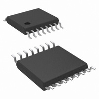
LM25088MH-1/NOPB National Semiconductor, LM25088MH-1/NOPB Datasheet - Page 6

LM25088MH-1/NOPB
Manufacturer Part Number
LM25088MH-1/NOPB
Description
IC CTLR BUCK NON-SYNC 16-TSSOP
Manufacturer
National Semiconductor
Series
PowerWise®r
Type
Step-Down (Buck)r
Datasheet
1.LM25088MH-2NOPB.pdf
(28 pages)
Specifications of LM25088MH-1/NOPB
Design Resources
LM(2)5088-1/2 QS Component Calculator
Internal Switch(s)
No
Synchronous Rectifier
No
Number Of Outputs
1
Voltage - Output
1.21 ~ 45 V
Current - Output
10A
Frequency - Switching
200kHz, 500kHz
Voltage - Input
4.5 ~ 42 V
Operating Temperature
-40°C ~ 125°C
Mounting Type
Surface Mount
Package / Case
16-TSSOP Exposed Pad, 16-eTSSOP, 16-HTSSOP
Primary Input Voltage
42V
No. Of Outputs
1
Output Voltage
1.2V
Output Current
10A
No. Of Pins
16
Operating Temperature Range
-40°C To +125°C
Msl
MSL 1 - Unlimited
Filter Terminals
SMD
Rohs Compliant
Yes
Lead Free Status / RoHS Status
Lead free / RoHS Compliant
Power - Output
-
Other names
LM25088MH-1
Available stocks
Company
Part Number
Manufacturer
Quantity
Price
Company:
Part Number:
LM25088MH-1/NOPB
Manufacturer:
NSC
Quantity:
800
www.national.com
OSCILLATOR (RT Pin)
SYNC
CURRENT LIMIT
CURRENT LIMIT RESTART (RES Pin)
RAMP GENERATOR
HIGH SIDE (HG) GATE DRIVER
THERMAL
Pre R
Note 1: Absolute Maximum Ratings are limits beyond which damage to the device may occur. Operating Ratings are conditions under which operation of the
device is intended to be functional. For guaranteed specifications and test conditions, see the Electrical Characteristics.
Note 2: The human body model is a 100 pF capacitor discharged through a 1.5 kΩ resistor into each pin.
Note 3: RAMP and COMP are output pins. As such they are not specified to have an external voltage applied.
Note 4: Typical specifications represent the most likely parametric norm at 25°C operation.
Note 5: For detailed information on soldering plastic MSOP packages refer to the Packaging Data Book available from National Semiconductor Corporation.
I
Symbol
V
I
V
rampdown
discharge
I
I
F
F
V
I
V
RAMP1
RAMP2
V
F
resdown
charge
I
F
CS(TH)
I
T
θ
OHH
θ
nom1
nom2
resup
OLH
OHH
max
OLH
min
SD
JC
JA
DS(ON)
Parameter
Nominal Oscillator Frequency
Dithering Range
SYNC positive threshold
SYNC Pulse Width
Cycle by cycle sense voltage threshold V
Cycle by Cycle Current Limit Delay
Buck Switch VDS protection
RES Threshold Upper (rising)
RES Threshold Lower (falling)
Charge source current
Discharge sink current
Discharge sink current -(post fault)
RAMP Current 1
RAMP Current 2
VOUT Bias Current
RAMP Output Low Voltage
HG Low-state Output Voltage
HG High-state Output Voltage
HG Rise Time
HG Fall Time
Peak HG Source Current
Peak HG Sink Current
BOOT UVLO
Pre-Charge Switch ON- resistance
Pre-Charge switch ON time
Thermal Shutdown Temperature
Thermal Shutdown Hysterisis
Thermal Resistance
Thermal Resistance
Conditions
LM25088-2 (Non-Dithering)
R
R
LM25088-1 (Dithering)
Minimum Dither Frequency
Maximum Dither Frequency
V
VIN to SW
V
V
V
V
V
V
V
I
I
C
C
V
V
BOOT to SW
I
Junction Temperature Rising
Junction Temperature Falling
Junction to Case
Junction to Ambient
HG
HG
VCC
RT
RT
RAMP
RAMP
CS
CS
CS
VIN
VIN
OUT
VIN
load
load
HG
HG
= 100 mA
= -100 mA, V
=31.6 kΩ
= 11.3 kΩ
= 0.125
>= 0.125
< 0.125
= 0V
= V
= 1 mA
= 36V, V
= 10V, V
= 36V, V
= 1000 pF
= 1000 pF
= 24V
= 0V
= 2.5V
VCC
6
OUT
OUT
OUT
OHH
= 10V
= 10V
= 10V
= V
BOOT
- V
HG
Min
180
430
112
135
1.1
0.1
0.8
15
40
20
18
F
F
nom
nom
Typ
200
500
120
280
165
125
200
115
240
300
165
2.3
1.5
1.2
0.2
1.2
1.5
50
27
25
12
72
25
40
6
2
3
6
+5%
-5%
Max
220
565
150
136
195
215
1.3
0.3
1.6
65
34
30
°C /W
°C /W
Units
kHz
kHz
kHz
kHz
mV
mV
mV
mV
µA
µA
µA
µA
µA
µA
°C
°C
ns
ns
ns
ns
ns
V
V
V
V
A
A
V
Ω


