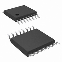
LM25088MH-1/NOPB National Semiconductor, LM25088MH-1/NOPB Datasheet - Page 21

LM25088MH-1/NOPB
Manufacturer Part Number
LM25088MH-1/NOPB
Description
IC CTLR BUCK NON-SYNC 16-TSSOP
Manufacturer
National Semiconductor
Series
PowerWise®r
Type
Step-Down (Buck)r
Datasheet
1.LM25088MH-2NOPB.pdf
(28 pages)
Specifications of LM25088MH-1/NOPB
Design Resources
LM(2)5088-1/2 QS Component Calculator
Internal Switch(s)
No
Synchronous Rectifier
No
Number Of Outputs
1
Voltage - Output
1.21 ~ 45 V
Current - Output
10A
Frequency - Switching
200kHz, 500kHz
Voltage - Input
4.5 ~ 42 V
Operating Temperature
-40°C ~ 125°C
Mounting Type
Surface Mount
Package / Case
16-TSSOP Exposed Pad, 16-eTSSOP, 16-HTSSOP
Primary Input Voltage
42V
No. Of Outputs
1
Output Voltage
1.2V
Output Current
10A
No. Of Pins
16
Operating Temperature Range
-40°C To +125°C
Msl
MSL 1 - Unlimited
Filter Terminals
SMD
Rohs Compliant
Yes
Lead Free Status / RoHS Status
Lead free / RoHS Compliant
Power - Output
-
Other names
LM25088MH-1
Available stocks
Company
Part Number
Manufacturer
Quantity
Price
Company:
Part Number:
LM25088MH-1/NOPB
Manufacturer:
NSC
Quantity:
800
PCB BOARD LAYOUT AND THERMAL
CONSIDERATIONS
In a buck regulator there are two loops where currents are
switched very fast. The first loop starts from the input capac-
itors, through the buck MOSFET, to the inductor then out to
the load. The second loop starts from the output capacitor
ground, to the regulator PGND pins, to the current sense re-
sistor, through the Schottky diode, to the inductor and then
out to the load. Minimizing the area of these two loops reduces
the stray inductance and minimizes noise which can cause
erratic operation. A ground plane is recommended as a
means to connect the input filter capacitors of the output filter
capacitors and the PGND pin of the regulator. Connect all of
the low power ground connections (C
to the regulator GND pin. Connect the GND pin and PGND
pins together through to topside copper area covering the en-
tire underside of the device. Place several vias in this under-
side copper area to the ground plane. The input capacitor
ground connection should be as close as possible to the cur-
rent sense ground connection.
In a buck converter, most of the losses can be attributed to
MOSFET conduction and switching loss, re-circulating diode
conduction loss, inductor DCR loss and LM25088 VIN and
VCC loss. The other dissipative components in a buck con-
SS
, R
T
, C
RAMP
) directly
21
verter produce losses but these other losses collectively ac-
count for about 2% of the total loss. Formulae to calculate all
the major losses are described in their respective sections of
this datasheet. The easiest method to determine the power
dissipated within the LM25088 is to measure the total con-
version losses (Pin-Pout), then subtract the power losses in
the Schottky diode, MOSFET, output inductor and snubber
resistor. When operating at 7A of output current and at 36V,
the power dissipation of the LM25088 is approximately 550
mW. The junction to ambient thermal resistance of the
LM25088 mounted in the evaluation board is approximately
40°C with no airflow. At 25°C ambient temperature and no
airflow, the predicted junction temperature will be 25+40*0.55
= 47°C. The LM25088 has an exposed thermal pad to aid in
power dissipation. Adding several vias under the device will
greatly reduce the controller junction temperature. The junc-
tion to ambient thermal resistance will vary with application.
The most significant variables are the area of copper in the
PC board; the number of vias under the IC exposed pad and
the amount of forced air cooling. The integrity of solder con-
nection from the IC exposed pad to the PC board is critical.
Excessive voids will greatly diminish the thermal dissipation
capacity.
www.national.com


