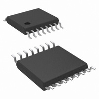
LM25088MH-1/NOPB National Semiconductor, LM25088MH-1/NOPB Datasheet - Page 5

LM25088MH-1/NOPB
Manufacturer Part Number
LM25088MH-1/NOPB
Description
IC CTLR BUCK NON-SYNC 16-TSSOP
Manufacturer
National Semiconductor
Series
PowerWise®r
Type
Step-Down (Buck)r
Datasheet
1.LM25088MH-2NOPB.pdf
(28 pages)
Specifications of LM25088MH-1/NOPB
Design Resources
LM(2)5088-1/2 QS Component Calculator
Internal Switch(s)
No
Synchronous Rectifier
No
Number Of Outputs
1
Voltage - Output
1.21 ~ 45 V
Current - Output
10A
Frequency - Switching
200kHz, 500kHz
Voltage - Input
4.5 ~ 42 V
Operating Temperature
-40°C ~ 125°C
Mounting Type
Surface Mount
Package / Case
16-TSSOP Exposed Pad, 16-eTSSOP, 16-HTSSOP
Primary Input Voltage
42V
No. Of Outputs
1
Output Voltage
1.2V
Output Current
10A
No. Of Pins
16
Operating Temperature Range
-40°C To +125°C
Msl
MSL 1 - Unlimited
Filter Terminals
SMD
Rohs Compliant
Yes
Lead Free Status / RoHS Status
Lead free / RoHS Compliant
Power - Output
-
Other names
LM25088MH-1
Available stocks
Company
Part Number
Manufacturer
Quantity
Price
Company:
Part Number:
LM25088MH-1/NOPB
Manufacturer:
NSC
Quantity:
800
VIN SUPPLY
VCC REGULATOR
ENABLE THRESHOLDS
SOFT- START
ERROR AMPLIFIER
PWM COMPARATORS
VIN, VOUT to GND
BOOT to GND
SW to GND
VCC to GND
HG to SW
EN to GND
BOOT to SW
I
Absolute Maximum Ratings
If Military/Aerospace specified devices are required,
please contact the National Semiconductor Sales Office/
Distributors for availability and specifications.
Electrical Characteristics
junction temperature (T
correlation. Typical values represent at T
following conditions apply: V
SHUTDOWN
V
V
Symbol
I
V
T
T
STANDBY
VCC(Reg)
VCC(Reg)
HG(OFF)
VCC(UV)
FBW
ON(MIN)
V
AOL
I
BIAS
REF
Parameter
VIN Operating Current
VIN Standby Current
VIN Shutdown Current
VCC Regulation
VCC Regulation
VCC Sourcing Current Limit
VCC Under-Voltage Lockout Threshold Positive going VVCC
VCC Under-Voltage Hysteresis
EN Shutdown Threshold
EN Shutdown Hysteresis
EN Standby Threshold
EN Standby Hysteresis
EN Pull-up Current Source
SS Pull-up Current Source
FB to SS Offset
FB Reference Voltage
FB Input Bias Current
COMP Sink/Source Current
DC Gain
Unity gain bandwidth
Forced HG Off-time
Minimum HG On-time
COMP to PWM comparator offset
J
) range of -40°C to +125°C. Minimum and Maximum limits are guaranteed through test, design, or statistical
VIN
= 24V, V
VCC
J
= 25°C, and are provided for reference purposes only. Unless otherwise stated the
= 8V, V
Limits in standard type are for T
-0.3V to BOOT
(Note
-0.3V to 16V
-0.3V to 16V
-2V to 45V
EN
)
Conditions
V
V
V
V
V
V
V
V
V
V
V
V
V
Measured at FB Pin
FB = COMP
V
V
+0.3V
= 5V R
FB
EN
EN
VCC
VIN
VCC
EN
EN
EN
EN
EN
SS
FB
FB
VIN
45V
60V
14V
= 1.3V
= 0V
= 1.3V
= 1.2V
= 1V
= 0V
Rising
Falling
Rising
Falling
= 0V
= 4.5V,VVCC=open
= 36V
= open
= 0
RT
5
= 31.6 kΩ, No load on HG. See Note 4.
CS, CSG to GND
All other inputs to GND
ESD Rating
Storage Temperature Range
Junction Temperature
VIN Voltage
VCC Voltage (externally supplied)
Operation Junction Temperature
Operating Ratings
Human Body Model
J
= 25°C only; limits in boldface type apply over the
1.187
Min
320
185
7.4
4.3
3.7
1.1
25
8
3
(Note
1.205
Typ
200
400
100
120
150
280
930
3.2
2.5
7.8
1.2
14
30
11
18
60
55
4
5
3
)
−40°C to + 125°C
−65°C to + 150°C
-0.3V to 0.3V
1.223
Max
480
100
365
www.national.com
4.5
3.0
8.2
4.5
4.2
1.3
4.5V to 42V
8.3V to 13V
24
13
-0.3V to 7V
+ 150°C
2 kV
Units
MHz
mA
mA
mA
mV
mV
mV
mV
mV
mA
mV
µA
µA
µA
nA
dB
ns
ns
V
V
V
V
V


