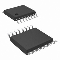
LM25088MH-1/NOPB National Semiconductor, LM25088MH-1/NOPB Datasheet - Page 3

LM25088MH-1/NOPB
Manufacturer Part Number
LM25088MH-1/NOPB
Description
IC CTLR BUCK NON-SYNC 16-TSSOP
Manufacturer
National Semiconductor
Series
PowerWise®r
Type
Step-Down (Buck)r
Datasheet
1.LM25088MH-2NOPB.pdf
(28 pages)
Specifications of LM25088MH-1/NOPB
Design Resources
LM(2)5088-1/2 QS Component Calculator
Internal Switch(s)
No
Synchronous Rectifier
No
Number Of Outputs
1
Voltage - Output
1.21 ~ 45 V
Current - Output
10A
Frequency - Switching
200kHz, 500kHz
Voltage - Input
4.5 ~ 42 V
Operating Temperature
-40°C ~ 125°C
Mounting Type
Surface Mount
Package / Case
16-TSSOP Exposed Pad, 16-eTSSOP, 16-HTSSOP
Primary Input Voltage
42V
No. Of Outputs
1
Output Voltage
1.2V
Output Current
10A
No. Of Pins
16
Operating Temperature Range
-40°C To +125°C
Msl
MSL 1 - Unlimited
Filter Terminals
SMD
Rohs Compliant
Yes
Lead Free Status / RoHS Status
Lead free / RoHS Compliant
Power - Output
-
Other names
LM25088MH-1
Available stocks
Company
Part Number
Manufacturer
Quantity
Price
Company:
Part Number:
LM25088MH-1/NOPB
Manufacturer:
NSC
Quantity:
800
Pin(S)
Pin Descriptions
10
10
11
12
13
14
1
2
3
4
5
6
7
8
9
RT/SYNC
COMP
RAMP
Name
DITH
GND
OUT
CSG
RES
VIN
SW
HG
EN
SS
FB
CS
Internal oscillator frequency
Output of the internal error
Output voltage connection Connect directly to the regulated output voltage.
Feedback signal from the
Current Sense Ground
synchronization input
Hiccup Mode Restart
Frequency Dithering
Input supply voltage
Ramp control signal
( LM25088-1 Only)
( LM25088-2 Only)
regulated output
Switching node
Current sense
set input and
Enable input
Description
High Gate
Soft-start
amplifier
Ground
Application Information
IC supply voltage. The operating range is 4.5V to 42V.
If the EN pin voltage is below 0.4V the regulator will be in a low power state. If
the EN pin voltage is between 0.4V and 1.2V the controller will be in standby
mode. If the EN pin voltage is above 1.2V the controller will be operational. An
external voltage divider can be used to set a line under voltage shutdown
threshold. If the EN pin is left open, a 5µA pull-up current forces the pin to the
high state and enables the controller.
When SS is below the internal 1.2V reference, the SS voltage will control the
error amplifier. An internal 11 µA current source charges an external capacitor
to set the start-up rate of the controller. The SS pin is held low in the standby,
VCC UV and thermal shutdown states. The SS pin can be used for voltage
tracking by connecting this pin to a master voltage supply less than 1.2V. The
applied voltage will act as the reference for the error amplifier.
An external capacitor connected between this pin and the GND pin sets the
ramp slope used for emulated current mode control. Recommended capacitor
range 100 pF to 2000 pF. See the Applications section for selection of capacitor
value.
The internal oscillator is programmed with a single resistor between this pin
and the GND pin. The recommended frequency range is 50 kHz to 1 MHz. An
external synchronization signal, which is higher in frequency than the
programmed frequency, can be applied to this pin through a small coupling
capacitor. The RT resistor to ground is required even when using external
synchronization.
Ground return.
The loop compensation network should be connected between this pin and the
FB pin.
This pin is connected to the inverting input of the internal error amplifier. The
regulation threshold is 1.205V.
A capacitor connected between DITH pin and GND is charged and discharged
by 27 µA current sources. As the voltage on the DITH pin ramps up and down,
the oscillator frequency is modulated between -5% to +5% of the nominal
frequency set by the RT resistor. Grounding the DITH pin will disable the
frequency dithering mode.
The RES pin is normally connected to an external capacitor that sets the timing
for hiccup mode current limiting. In normal operation, a 25 µA current source
discharges the RES pin capacitor to ground. If cycle-by-cycle current limit
threshold is exceeded during any PWM cycle, the current sink is disabled and
RES capacitor is charged by an internal 50 µA current. If the RES voltage
reaches 1.2V, the HG pin gate drive signal will be disabled and the RES pin
capacitor will be discharged by a 1 µA current sink. Normal operation will
resume when the RES pin falls below 0.2V.
Low side reference for the current sense resistor.
Current measurement connection for the re-circulating diode. An external
sense resistor and an internal sample/hold circuit sense the diode current at
the conclusion of the buck switch off-time. This current measurement provides
the DC offset level for the emulated current ramp.
Connect to the source terminal of the external MOSFET switch.
Connect to the gate terminal of the external MOSFET switch.
3
www.national.com


