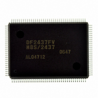
DF2437FV Renesas Electronics America, DF2437FV Datasheet - Page 290

DF2437FV
Manufacturer Part Number
DF2437FV
Description
IC H8S/2437 MCU FLASH 128QFP
Manufacturer
Renesas Electronics America
Series
H8® H8S/2400r
Specifications of DF2437FV
Core Processor
H8S/2600
Core Size
16-Bit
Speed
20MHz
Connectivity
I²C, SCI
Peripherals
POR, PWM, WDT
Number Of I /o
85
Program Memory Size
256KB (256K x 8)
Program Memory Type
FLASH
Ram Size
16K x 8
Voltage - Supply (vcc/vdd)
3 V ~ 3.6 V
Data Converters
A/D 16x10b
Oscillator Type
Internal
Operating Temperature
-20°C ~ 75°C
Package / Case
128-QFP
Lead Free Status / RoHS Status
Lead free / RoHS Compliant
Eeprom Size
-
Available stocks
Company
Part Number
Manufacturer
Quantity
Price
Company:
Part Number:
DF2437FV
Manufacturer:
Renesas Electronics America
Quantity:
10 000
- Current page: 290 of 776
- Download datasheet (5Mb)
• Timer interrupt enable register (TIER)
• Timer control/status register (TCSR)
• Timer control register (TCR)
• Timer output compare control register (TOCR)
Note: OCRA_0 (OCRA_1) and OCRB_0 (OCRB_1) share the same address. Register selection
10.3.1
FRC is a 16-bit readable/writable up-counter. The clock source is selected by bits CKS1 and
CKS0 in TCR. FRC can be cleared by compare-match A. When FRC overflows from H'FFFF to
H'0000, the OVF flag in TCSR is set to 1. FRC should always be accessed in 16-bit units; cannot
be accessed in 8-bit units. FRC is initialized to H'0000.
10.3.2
The FRT has two output compare registers, OCRA and OCRB, each of which is a 16-bit
readable/writable register whose contents are continually compared with the value in FRC. When
a match is detected (compare-match), the OCFA or OCFB flag in TCSR is set to 1. If the OEA or
OEB bit in TOCR is set to 1, when the OCR and FRC values match, the output level selected by
the OLVLA or OLVLB bit in TOCR is output at the output compare output pin (FTOA or FTOB).
Following a reset, the FTOA and FTOB output levels are 0 until the first compare-match. OCR
should always be accessed in 16-bit units; cannot be accessed in 8-bit units. OCR is initialized to
H'FFFF.
10.3.3
The FRT has four input capture registers, ICRA to ICRD, each of which is a 16-bit read-only
register. When the rising or falling edge of the signal at an input capture input pin (FTIA to FTID)
is detected, the current FRC value is transferred to ICRA to ICRD. At the same time, the ICFA to
ICFD flags in TCSR are set to 1. The FRC contents are transferred to ICR regardless of the value
of ICF. The input capture edge is selected by the IEDGA to IEDGD bits in TCR.
ICRC and ICRD can be used as ICRA and ICRB buffer registers, respectively, by means of the
BUFEA and BUFEB bits in TCR.
Rev.2.00 May. 28, 2009 Page 250 of 732
REJ09B0059-0200
is controlled by the OCRS bit in TOCR_0 (TOCR_1). ICRA_0 (ICRA_1), ICRB_0
(ICRB_1), and ICRC_0 (ICRC_1) share the same addresses with OCRAR_0 (OCRAR_1),
OCRAF_0 (OCRAF_1), and OCRDM_0 (OCRDM_1). Register selection is controlled by
the ICRS bit in TOCR_0 (TOCR_1).
Free-Running Counter (FRC)
Output Compare Registers A and B (OCRA and OCRB)
Input Capture Registers A to D (ICRA to ICRD)
Related parts for DF2437FV
Image
Part Number
Description
Manufacturer
Datasheet
Request
R

Part Number:
Description:
KIT STARTER FOR M16C/29
Manufacturer:
Renesas Electronics America
Datasheet:

Part Number:
Description:
KIT STARTER FOR R8C/2D
Manufacturer:
Renesas Electronics America
Datasheet:

Part Number:
Description:
R0K33062P STARTER KIT
Manufacturer:
Renesas Electronics America
Datasheet:

Part Number:
Description:
KIT STARTER FOR R8C/23 E8A
Manufacturer:
Renesas Electronics America
Datasheet:

Part Number:
Description:
KIT STARTER FOR R8C/25
Manufacturer:
Renesas Electronics America
Datasheet:

Part Number:
Description:
KIT STARTER H8S2456 SHARPE DSPLY
Manufacturer:
Renesas Electronics America
Datasheet:

Part Number:
Description:
KIT STARTER FOR R8C38C
Manufacturer:
Renesas Electronics America
Datasheet:

Part Number:
Description:
KIT STARTER FOR R8C35C
Manufacturer:
Renesas Electronics America
Datasheet:

Part Number:
Description:
KIT STARTER FOR R8CL3AC+LCD APPS
Manufacturer:
Renesas Electronics America
Datasheet:

Part Number:
Description:
KIT STARTER FOR RX610
Manufacturer:
Renesas Electronics America
Datasheet:

Part Number:
Description:
KIT STARTER FOR R32C/118
Manufacturer:
Renesas Electronics America
Datasheet:

Part Number:
Description:
KIT DEV RSK-R8C/26-29
Manufacturer:
Renesas Electronics America
Datasheet:

Part Number:
Description:
KIT STARTER FOR SH7124
Manufacturer:
Renesas Electronics America
Datasheet:

Part Number:
Description:
KIT STARTER FOR H8SX/1622
Manufacturer:
Renesas Electronics America
Datasheet:

Part Number:
Description:
KIT DEV FOR SH7203
Manufacturer:
Renesas Electronics America
Datasheet:


