DF2437FV Renesas Electronics America, DF2437FV Datasheet - Page 661
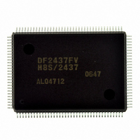
DF2437FV
Manufacturer Part Number
DF2437FV
Description
IC H8S/2437 MCU FLASH 128QFP
Manufacturer
Renesas Electronics America
Series
H8® H8S/2400r
Specifications of DF2437FV
Core Processor
H8S/2600
Core Size
16-Bit
Speed
20MHz
Connectivity
I²C, SCI
Peripherals
POR, PWM, WDT
Number Of I /o
85
Program Memory Size
256KB (256K x 8)
Program Memory Type
FLASH
Ram Size
16K x 8
Voltage - Supply (vcc/vdd)
3 V ~ 3.6 V
Data Converters
A/D 16x10b
Oscillator Type
Internal
Operating Temperature
-20°C ~ 75°C
Package / Case
128-QFP
Lead Free Status / RoHS Status
Lead free / RoHS Compliant
Eeprom Size
-
Available stocks
Company
Part Number
Manufacturer
Quantity
Price
Company:

Part Number:
DF2437FV
Manufacturer:
Renesas Electronics America
Quantity:
10 000


2. Multiplication Ratio
3. Operating Frequency
4. Bit Rate
When the new bit rate is selectable, the rate will be set in the register after sending ACK in
response. The host will send an ACK with the new bit rate for confirmation and the boot program
will response with that rate.
Confirmation
Response
The sequence of new bit-rate selection is shown in figure 20.22.
The received value of the multiplication ratio or division ratio is checked to ensure that it
matches the clock modes of the specified device. When the value is out of this range, a
multiplication-ratio error is generated.
Operating frequency is calculated from the received value of the input frequency and the
multiplication or division ratio. The input frequency is input to the LSI and the LSI is operated
at the operating frequency. The expression is given below.
Operating frequency = Input frequency × Multiplication ratio, or
Operating frequency = Input frequency ÷ Division ratio
The calculated operating frequency should be checked to ensure that it is within the range of
minimum to maximum frequencies which is available with the clock modes of the specified
device. When it is out of this range, an operating frequency error is generated.
The value (n) of the clock select bit (CKS) in the serial mode register (SMR), and the value
(N) in the bit rate register (BRR), which are found from the peripheral operating clock
frequency (φ) and bit rate (B), are used to calculate the error rate to ensure that it is less than
4%. If the error is more than 4%, a bit rate error is generated. The error is calculated using the
following expression:
• Confirmation, H'06, (one byte): Confirmation of a new bit rate
• Response, H'06, (one byte): Response to confirmation of a new bit rate
Error (%) = {[
H'06
H'06
(N + 1)
×
φ
B
×
×
10
64
6
×
2
(2×n − 1)
] − 1}
×
100
Rev.2.00 May. 28, 2009 Page 621 of 732
REJ09B0059-0200
Related parts for DF2437FV
Image
Part Number
Description
Manufacturer
Datasheet
Request
R

Part Number:
Description:
KIT STARTER FOR M16C/29
Manufacturer:
Renesas Electronics America
Datasheet:

Part Number:
Description:
KIT STARTER FOR R8C/2D
Manufacturer:
Renesas Electronics America
Datasheet:

Part Number:
Description:
R0K33062P STARTER KIT
Manufacturer:
Renesas Electronics America
Datasheet:

Part Number:
Description:
KIT STARTER FOR R8C/23 E8A
Manufacturer:
Renesas Electronics America
Datasheet:

Part Number:
Description:
KIT STARTER FOR R8C/25
Manufacturer:
Renesas Electronics America
Datasheet:

Part Number:
Description:
KIT STARTER H8S2456 SHARPE DSPLY
Manufacturer:
Renesas Electronics America
Datasheet:

Part Number:
Description:
KIT STARTER FOR R8C38C
Manufacturer:
Renesas Electronics America
Datasheet:

Part Number:
Description:
KIT STARTER FOR R8C35C
Manufacturer:
Renesas Electronics America
Datasheet:

Part Number:
Description:
KIT STARTER FOR R8CL3AC+LCD APPS
Manufacturer:
Renesas Electronics America
Datasheet:
Part Number:
Description:
KIT STARTER FOR RX610
Manufacturer:
Renesas Electronics America
Datasheet:

Part Number:
Description:
KIT STARTER FOR R32C/118
Manufacturer:
Renesas Electronics America
Datasheet:

Part Number:
Description:
KIT DEV RSK-R8C/26-29
Manufacturer:
Renesas Electronics America
Datasheet:

Part Number:
Description:
KIT STARTER FOR SH7124
Manufacturer:
Renesas Electronics America
Datasheet:

Part Number:
Description:
KIT STARTER FOR H8SX/1622
Manufacturer:
Renesas Electronics America
Datasheet:

Part Number:
Description:
KIT DEV FOR SH7203
Manufacturer:
Renesas Electronics America
Datasheet: