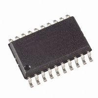
AT90PWM81-16SF Atmel, AT90PWM81-16SF Datasheet - Page 221

AT90PWM81-16SF
Manufacturer Part Number
AT90PWM81-16SF
Description
IC MCU AVR 8K FLASH ISP 20SOIC
Manufacturer
Atmel
Series
AVR® 90PWM Lightingr
Datasheet
1.AT90PWM81-16MN.pdf
(325 pages)
Specifications of AT90PWM81-16SF
Core Processor
AVR
Core Size
8-Bit
Speed
16MHz
Connectivity
SPI
Peripherals
Brown-out Detect/Reset, PWM, WDT
Number Of I /o
16
Program Memory Size
8KB (8K x 8)
Program Memory Type
FLASH
Eeprom Size
512 x 8
Ram Size
256 x 8
Voltage - Supply (vcc/vdd)
2.7 V ~ 5.5 V
Data Converters
A/D 8x10b; D/A 1x10b
Oscillator Type
Internal
Operating Temperature
-40°C ~ 105°C
Package / Case
20-SOIC (7.5mm Width)
For Use With
ATSTK600-SOIC - STK600 SOCKET/ADAPTER FOR SOIC
Lead Free Status / RoHS Status
Lead free / RoHS Compliant
Available stocks
Company
Part Number
Manufacturer
Quantity
Price
Company:
Part Number:
AT90PWM81-16SF
Manufacturer:
Atmel
Quantity:
2 428
- Current page: 221 of 325
- Download datasheet (6Mb)
17.8.4.2
17.8.5
17.8.6
17.9
7734P–AVR–08/10
Amplifier
Digital Input Disable Register 0 – DIDR0
Digital Input Disable Register 1– DIDR1
ADLAR = 1
• Bit 7:0 – ADC7D..ADC0D: AMP0-D and ADC7:0 Digital Input Disable
When this bit is written logic one, the digital input buffer on the corresponding ADC pin is disabled. The
corresponding PIN Register bit will always read as zero when this bit is set. When an analog signal is
applied to the ADC7..0 pin and the digital input from this pin is not needed, this bit should be written logic
one to reduce power consumption in the digital input buffer.
• Bit 2:0 – AMP0+D and ADC10:8 Digital Input Disable
When this bit is written logic one, the digital input buffer on the corresponding ADC pin is disabled. The
corresponding PIN Register bit will always read as zero when this bit is set. When an analog signal is
applied to an analog pin and the digital input from this pin is not needed, this bit should be written logic
one to reduce power consumption in the digital input buffer.
The AT90PWM81 features one differential amplified channel with programmable 5, 10, 20, and 40 gain
stage. Despite the result is given by the 10 bit ADC, the amplifier has been sized to give a 8bits resolution.
The negative input on the amplifier can be internally switched to the analog ground. However, amplifier
characteristics are specified with differential inputs.
Because the amplifier is a switching capacitor amplifier, it needs to be clocked by a synchronization signal
called in this document the amplifier synchronization clock. The amplifier samples the input value at the
falling edge of the synchronization signal. This allow to measure analog signals with same period as the
synchronization. The maximum clock for the amplifier is 250kHz.
Bit
Read/Write
Initial Value
Bit
Read/Write
Initial Value
Bit
Read/Write
Initial Value
7
ADC8D
AMP3D
R/W
0
7
-
-
0
7
ADC9
ADC1
R
R
0
0
6
ADC7D
AMP0-D
R/W
0
6
-
-
0
6
ADC8
ADC0
R
R
0
0
5
ADC5D
ACMP2D
R/W
0
5
-
R/W
0
5
ADC7
-
R
R
0
0
0
4
ADC4D
ACMP3MD
R/W
0
4
-
R/W
4
ADC6
-
R
R
0
0
3
ADC3D
ACMPMD
R/W
0
3
ACMP1MD AMP0+D
R/W
0
3
ADC5
-
R
R
0
0
2
ADC2D
ACMP2MD
R/W
0
2
R/W
0
2
ADC4
-
R
R
0
0
1
ADC1D
R/W
0
1
ADC10D
R/W
0
1
ADC3
-
R
R
0
0
AT90PWM81
0
ADC0D
ACMP1D
R/W
0
0
ADC9D
R/W
0
0
ADC2
-
R
R
0
0
DIDR0
DIDR1
ADCH
ADCL
221
Related parts for AT90PWM81-16SF
Image
Part Number
Description
Manufacturer
Datasheet
Request
R

Part Number:
Description:
Manufacturer:
Atmel Corporation
Datasheet:

Part Number:
Description:
IC MCU AVR 8K FLASH ISP 20SOIC
Manufacturer:
Atmel
Datasheet:

Part Number:
Description:
IC MCU AVR 8K FLASH ISP 32QFN
Manufacturer:
Atmel
Datasheet:

Part Number:
Description:
IC MCU AVR 8K FLASH ISP 32QFN
Manufacturer:
Atmel
Datasheet:

Part Number:
Description:
8-bit Avr Microcontroller With 8k Bytes In- System Programmable Flash
Manufacturer:
ATMEL Corporation
Datasheet:

Part Number:
Description:
DEV KIT FOR AVR/AVR32
Manufacturer:
Atmel
Datasheet:

Part Number:
Description:
INTERVAL AND WIPE/WASH WIPER CONTROL IC WITH DELAY
Manufacturer:
ATMEL Corporation
Datasheet:

Part Number:
Description:
Low-Voltage Voice-Switched IC for Hands-Free Operation
Manufacturer:
ATMEL Corporation
Datasheet:

Part Number:
Description:
MONOLITHIC INTEGRATED FEATUREPHONE CIRCUIT
Manufacturer:
ATMEL Corporation
Datasheet:

Part Number:
Description:
AM-FM Receiver IC U4255BM-M
Manufacturer:
ATMEL Corporation
Datasheet:

Part Number:
Description:
Monolithic Integrated Feature Phone Circuit
Manufacturer:
ATMEL Corporation
Datasheet:

Part Number:
Description:
Multistandard Video-IF and Quasi Parallel Sound Processing
Manufacturer:
ATMEL Corporation
Datasheet:


