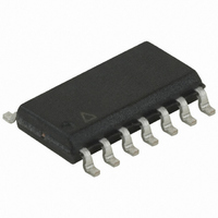
ATTINY24-15SSZ Atmel, ATTINY24-15SSZ Datasheet - Page 121

ATTINY24-15SSZ
Manufacturer Part Number
ATTINY24-15SSZ
Description
MCU AVR 2K FLASH 15MHZ 14-SOIC
Manufacturer
Atmel
Series
AVR® ATtinyr
Datasheet
1.ATTINY24-15SSZ.pdf
(225 pages)
Specifications of ATTINY24-15SSZ
Package / Case
14-SOIC (3.9mm Width), 14-SOL
Voltage - Supply (vcc/vdd)
2.7 V ~ 5.5 V
Operating Temperature
-40°C ~ 125°C
Speed
16MHz
Number Of I /o
12
Eeprom Size
128 x 8
Core Processor
AVR
Program Memory Type
FLASH
Ram Size
128 x 8
Program Memory Size
2KB (2K x 8)
Data Converters
A/D 8x10b
Oscillator Type
Internal
Peripherals
Brown-out Detect/Reset, POR, PWM, WDT
Connectivity
USI
Core Size
8-Bit
Cpu Family
ATtiny
Device Core
AVR
Device Core Size
8b
Frequency (max)
16MHz
Interface Type
SPI/UART
Total Internal Ram Size
128Byte
# I/os (max)
12
Number Of Timers - General Purpose
2
Operating Supply Voltage (typ)
3.3/5V
Operating Supply Voltage (max)
5.5V
Operating Supply Voltage (min)
2.7V
On-chip Adc
8-chx10-bit
Instruction Set Architecture
RISC
Operating Temp Range
-40C to 125C
Operating Temperature Classification
Automotive
Mounting
Surface Mount
Pin Count
14
Package Type
SOIC
Lead Free Status / RoHS Status
Lead free / RoHS Compliant
Available stocks
Company
Part Number
Manufacturer
Quantity
Price
Company:
Part Number:
ATTINY24-15SSZ
Manufacturer:
ATMEL
Quantity:
349
Part Number:
ATTINY24-15SSZ
Manufacturer:
ATTINY
Quantity:
20 000
- Current page: 121 of 225
- Download datasheet (4Mb)
16. USI – Universal Serial Interface
16.1
16.2
7701D–AVR–09/10
Features
Overview
•
•
•
•
•
•
The universal serial interface (USI) provides the basic hardware resources needed for serial
communication. Combined with a minimum of control software, the USI allows significantly
higher transfer rates and uses less code space than solutions based on software only. Inter-
rupts are included to minimize the processor load.
A simplified block diagram of the USI is shown in
placement of I/O pins, refer to
Registers, including I/O bits and I/O pins, are shown in bold. The device-specific I/O Register
and bit locations are listed in the
Figure 16-1. Universal Serial Interface, Block Diagram
The 8-bit shift register is directly accessible via the data bus and contains the incoming and
outgoing data. The register has no buffering, so the data must be read as quickly as possible
to ensure that no data are lost. The most significant bit is connected to one of two output pins,
depending on the wire mode configuration. A transparent latch is inserted between the serial
register output and output pin, which delays the change of data output to the opposite clock
edge of the data input sampling. The serial input is always sampled from the data input (DI)
pin independent of the configuration.
Two-wire Synchronous Data Transfer (Master or Slave)
Three-wire Synchronous Data Transfer (Master or Slave)
Data Received Interrupt
Wakeup from Idle Mode
In Two-wire Mode: Wakeup from All Sleep Modes, Including Power-down Mode
Two-wire Start Condition Detector with Interrupt Capability
USIDR
USISR
USICR
2
4-bit Counter
Atmel ATtiny24/44/84 [Preliminary]
“Pinout Atmel
“Register Descriptions” on page
3
2
1
0
3
2
1
0
D Q
LE
®
[1]
ATtiny24/44/84” on page
TIM0 COMP
0
1
Figure 16-1 on page
Two-wire Clock
Control Unit
129.
CLOCK
HOLD
2. CPU accessible I/O
121. For the actual
DO
DI/SDA
USCK/SCL
(Output only)
(Input/Open Drain)
(Input/Open Drain)
121
Related parts for ATTINY24-15SSZ
Image
Part Number
Description
Manufacturer
Datasheet
Request
R

Part Number:
Description:
Manufacturer:
Atmel Corporation
Datasheet:

Part Number:
Description:
Manufacturer:
Atmel Corporation
Datasheet:

Part Number:
Description:
IC MCU AVR 2K FLASH 20MHZ 20-QFN
Manufacturer:
Atmel
Datasheet:

Part Number:
Description:
IC MCU AVR 2K FLASH 20MHZ 14SOIC
Manufacturer:
Atmel
Datasheet:

Part Number:
Description:
MCU AVR 2K FLASH 15MHZ 20-QFN
Manufacturer:
Atmel
Datasheet:

Part Number:
Description:
IC MCU AVR 2K FLASH 20MHZ 14-DIP
Manufacturer:
Atmel
Datasheet:

Part Number:
Description:
MCU AVR 2KB FLASH 20MHZ 14SOIC
Manufacturer:
Atmel
Datasheet:

Part Number:
Description:
MCU AVR 2KB FLASH 20MHZ 20QFN
Manufacturer:
Atmel
Datasheet:

Part Number:
Description:
IC, MCU, 8BIT, 2K FLASH, 20SOIC
Manufacturer:
Atmel
Datasheet:

Part Number:
Description:
IC, MCU, 8BIT, 2K FLASH, 20PDIP
Manufacturer:
Atmel
Datasheet:

Part Number:
Description:
IC, MCU, 8BIT, 8K FLASH, 20PDIP
Manufacturer:
Atmel
Datasheet:

Part Number:
Description:
IC, MCU, 8BIT, 8K FLASH, 20SOIC
Manufacturer:
Atmel
Datasheet:


