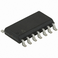
ATTINY24-15SSZ Atmel, ATTINY24-15SSZ Datasheet - Page 138

ATTINY24-15SSZ
Manufacturer Part Number
ATTINY24-15SSZ
Description
MCU AVR 2K FLASH 15MHZ 14-SOIC
Manufacturer
Atmel
Series
AVR® ATtinyr
Datasheet
1.ATTINY24-15SSZ.pdf
(225 pages)
Specifications of ATTINY24-15SSZ
Package / Case
14-SOIC (3.9mm Width), 14-SOL
Voltage - Supply (vcc/vdd)
2.7 V ~ 5.5 V
Operating Temperature
-40°C ~ 125°C
Speed
16MHz
Number Of I /o
12
Eeprom Size
128 x 8
Core Processor
AVR
Program Memory Type
FLASH
Ram Size
128 x 8
Program Memory Size
2KB (2K x 8)
Data Converters
A/D 8x10b
Oscillator Type
Internal
Peripherals
Brown-out Detect/Reset, POR, PWM, WDT
Connectivity
USI
Core Size
8-Bit
Cpu Family
ATtiny
Device Core
AVR
Device Core Size
8b
Frequency (max)
16MHz
Interface Type
SPI/UART
Total Internal Ram Size
128Byte
# I/os (max)
12
Number Of Timers - General Purpose
2
Operating Supply Voltage (typ)
3.3/5V
Operating Supply Voltage (max)
5.5V
Operating Supply Voltage (min)
2.7V
On-chip Adc
8-chx10-bit
Instruction Set Architecture
RISC
Operating Temp Range
-40C to 125C
Operating Temperature Classification
Automotive
Mounting
Surface Mount
Pin Count
14
Package Type
SOIC
Lead Free Status / RoHS Status
Lead free / RoHS Compliant
Available stocks
Company
Part Number
Manufacturer
Quantity
Price
Company:
Part Number:
ATTINY24-15SSZ
Manufacturer:
ATMEL
Quantity:
349
Part Number:
ATTINY24-15SSZ
Manufacturer:
ATTINY
Quantity:
20 000
If differential channels are selected, the differential gain stage amplifies the voltage difference
between the selected input pair by the selected gain factor, 1x or 20x, according to the setting
of the MUX0 bit in the ADMUX register. This amplified value then becomes the analog input to
the ADC. If single-ended channels are used, the gain amplifier is bypassed altogether.
The offset of the differential channels can be measure by selecting the same input for both
negative and positive input. Offset calibration can be done for ADC0, ADC3 and ADC7. When
ADC0, ADC3, or ADC7 is selected as both the positive and negative input to the differential
gain amplifier, the remaining offset in the gain stage and conversion circuitry can be measured
directly as the result of the conversion. This figure can be subtracted from subsequent conver-
sions with the same gain setting to reduce offset error to below 1 LSB.
The on-chip temperature sensor is selected by writing "100010" to the MUX5..0 bits in the
ADMUX register.
The ADC is enabled by setting the ADC enable bit (ADEN) in ADCSRA. Voltage reference and
input channel selections will not go into effect until ADEN is set. The ADC does not consume
power when ADEN is cleared, so it is recommended to switch off the ADC before entering
power saving sleep modes.
The ADC generates a 10-bit result which is presented in the ADC data registers, ADCH and
ADCL. By default, the result is presented right adjusted, but can optionally be presented left
adjusted by setting the ADLAR bit in ADCSRB.
If the result is left adjusted and no more than 8-bit precision is required, it is sufficient to read
ADCH. Otherwise, ADCL must be read first, then ADCH, to ensure that the content of the data
registers belongs to the same conversion. Once ADCL is read, ADC access to data registers
is blocked. This means that if ADCL has been read, and a conversion completes before ADCH
is read, neither register is updated, and the result from the conversion is lost. When ADCH is
read, ADC access to the ADCH and ADCL registers is re-enabled.
The ADC has its own interrupt which can be triggered when a conversion completes. When
ADC access to the data registers is prohibited between reading of ADCH and ADCL, the inter-
rupt will trigger even if the result is lost.
18.4
Starting a Conversion
A single conversion is started by writing a logical one to the ADC start conversion bit, ADSC.
This bit stays high as long as the conversion is in progress, and will be cleared by hardware
when the conversion is completed. If a different data channel is selected while a conversion is
in progress, the ADC will finish the current conversion before performing the channel change.
Alternatively, a conversion can be triggered automatically by various sources. Auto triggering
is enabled by setting the ADC auto trigger enable bit (ADATE) in ADCSRA. The trigger source
is selected by setting the ADC trigger select bits (ADTS) in ADCSRB (see the description of
the ADTS bits for a list of the trigger sources). When a positive edge occurs on the selected
trigger signal, the ADC prescaler is reset and a conversion is started. This provides a method
of starting conversions at fixed intervals. If the trigger signal still is set when the conversion
completes, a new conversion will not be started. If another positive edge occurs on the trigger
signal during conversion, the edge will be ignored. Note that an interrupt flag will be set even if
the specific interrupt is disabled or the global interrupt enable bit in SREG is cleared. A conver-
sion can thus be triggered without causing an interrupt. However, the Interrupt Flag must be
cleared in order to trigger a new conversion at the next interrupt event
.
Atmel ATtiny24/44/84 [Preliminary]
138
7701D–AVR–09/10


