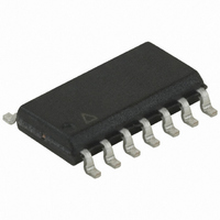
ATTINY24-15SSZ Atmel, ATTINY24-15SSZ Datasheet - Page 37

ATTINY24-15SSZ
Manufacturer Part Number
ATTINY24-15SSZ
Description
MCU AVR 2K FLASH 15MHZ 14-SOIC
Manufacturer
Atmel
Series
AVR® ATtinyr
Datasheet
1.ATTINY24-15SSZ.pdf
(225 pages)
Specifications of ATTINY24-15SSZ
Package / Case
14-SOIC (3.9mm Width), 14-SOL
Voltage - Supply (vcc/vdd)
2.7 V ~ 5.5 V
Operating Temperature
-40°C ~ 125°C
Speed
16MHz
Number Of I /o
12
Eeprom Size
128 x 8
Core Processor
AVR
Program Memory Type
FLASH
Ram Size
128 x 8
Program Memory Size
2KB (2K x 8)
Data Converters
A/D 8x10b
Oscillator Type
Internal
Peripherals
Brown-out Detect/Reset, POR, PWM, WDT
Connectivity
USI
Core Size
8-Bit
Cpu Family
ATtiny
Device Core
AVR
Device Core Size
8b
Frequency (max)
16MHz
Interface Type
SPI/UART
Total Internal Ram Size
128Byte
# I/os (max)
12
Number Of Timers - General Purpose
2
Operating Supply Voltage (typ)
3.3/5V
Operating Supply Voltage (max)
5.5V
Operating Supply Voltage (min)
2.7V
On-chip Adc
8-chx10-bit
Instruction Set Architecture
RISC
Operating Temp Range
-40C to 125C
Operating Temperature Classification
Automotive
Mounting
Surface Mount
Pin Count
14
Package Type
SOIC
Lead Free Status / RoHS Status
Lead free / RoHS Compliant
Available stocks
Company
Part Number
Manufacturer
Quantity
Price
Company:
Part Number:
ATTINY24-15SSZ
Manufacturer:
ATMEL
Quantity:
349
Part Number:
ATTINY24-15SSZ
Manufacturer:
ATTINY
Quantity:
20 000
- Current page: 37 of 225
- Download datasheet (4Mb)
8.7.6
8.8
8.8.1
7701D–AVR–09/10
Register Description
Port Pins
MCUCR – MCU Control Register
When entering a sleep mode, all port pins should be configured to use minimum power. The
most important thing is then to ensure that no pins drive resistive loads. In sleep modes where
both the I/O clock (clk
device will be disabled. This ensures that no power is consumed by the input logic when not
needed. In some cases, the input logic is needed for detecting wake-up conditions, and it will
then be enabled. See the section
details on which pins are enabled. If the input buffer is enabled and the input signal is left float-
ing or has an analog signal level close to V
For analog input pins, the digital input buffer should be disabled at all times. An analog signal
level close to V
input buffers can be disabled by writing to the Digital Input Disable Register (DIDR0). See
“DIDR0 – Digital Input Disable Register 0” on page 154
The MCU Control Register contains control bits for power management.
• Bit 5 – SE: Sleep Enable
The SE bit must be written to logical one to make the MCU enter the sleep mode when the
SLEEP instruction is executed. To avoid the MCU entering the sleep mode unless it is the pro-
grammer's purpose, it is recommended to set the sleep enable (SE) bit just before the
execution of the SLEEP instruction and to clear it immediately after waking up.
• Bits 4, 3 – SM1..0: Sleep Mode Select Bits 2..0
These bits select between the three available sleep modes as shown in
Table 8-2.
Note:
• Bit 2 – Res: Reserved Bit
This bit is a reserved bit in the Atmel
Bit
Read/Write
Initial Value
SM1
1. Only recommended with external crystal or resonator selected as clock source
0
0
1
1
Sleep Mode Select
CC
R
7
–
0
/2 on an input pin can cause significant current even in active mode. Digital
I/O
PUD
R/W
SM0
) and the ADC clock (clk
6
0
0
1
0
1
Atmel ATtiny24/44/84 [Preliminary]
R/W
SE
5
0
“Digital Input Enable and Sleep Modes” on page 59
®
Sleep Mode
Idle
ADC Noise Reduction
Power-down
Standby
ATtiny24/44/84 and will always read as zero.
SM1
R/W
CC
4
0
(1)
/2, the input buffer will use excessive power.
ADC
SM0
R/W
3
0
) are stopped, the input buffers of the
for details.
—
R
2
0
ISC01
R/W
1
0
Table 8-2 on page
ISC00
R/W
0
0
MCUCR
37.
for
37
Related parts for ATTINY24-15SSZ
Image
Part Number
Description
Manufacturer
Datasheet
Request
R

Part Number:
Description:
Manufacturer:
Atmel Corporation
Datasheet:

Part Number:
Description:
Manufacturer:
Atmel Corporation
Datasheet:

Part Number:
Description:
IC MCU AVR 2K FLASH 20MHZ 20-QFN
Manufacturer:
Atmel
Datasheet:

Part Number:
Description:
IC MCU AVR 2K FLASH 20MHZ 14SOIC
Manufacturer:
Atmel
Datasheet:

Part Number:
Description:
MCU AVR 2K FLASH 15MHZ 20-QFN
Manufacturer:
Atmel
Datasheet:

Part Number:
Description:
IC MCU AVR 2K FLASH 20MHZ 14-DIP
Manufacturer:
Atmel
Datasheet:

Part Number:
Description:
MCU AVR 2KB FLASH 20MHZ 14SOIC
Manufacturer:
Atmel
Datasheet:

Part Number:
Description:
MCU AVR 2KB FLASH 20MHZ 20QFN
Manufacturer:
Atmel
Datasheet:

Part Number:
Description:
IC, MCU, 8BIT, 2K FLASH, 20SOIC
Manufacturer:
Atmel
Datasheet:

Part Number:
Description:
IC, MCU, 8BIT, 2K FLASH, 20PDIP
Manufacturer:
Atmel
Datasheet:

Part Number:
Description:
IC, MCU, 8BIT, 8K FLASH, 20PDIP
Manufacturer:
Atmel
Datasheet:

Part Number:
Description:
IC, MCU, 8BIT, 8K FLASH, 20SOIC
Manufacturer:
Atmel
Datasheet:


