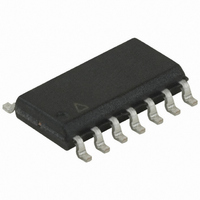
ATTINY24-15SSZ Atmel, ATTINY24-15SSZ Datasheet - Page 65

ATTINY24-15SSZ
Manufacturer Part Number
ATTINY24-15SSZ
Description
MCU AVR 2K FLASH 15MHZ 14-SOIC
Manufacturer
Atmel
Series
AVR® ATtinyr
Datasheet
1.ATTINY24-15SSZ.pdf
(225 pages)
Specifications of ATTINY24-15SSZ
Package / Case
14-SOIC (3.9mm Width), 14-SOL
Voltage - Supply (vcc/vdd)
2.7 V ~ 5.5 V
Operating Temperature
-40°C ~ 125°C
Speed
16MHz
Number Of I /o
12
Eeprom Size
128 x 8
Core Processor
AVR
Program Memory Type
FLASH
Ram Size
128 x 8
Program Memory Size
2KB (2K x 8)
Data Converters
A/D 8x10b
Oscillator Type
Internal
Peripherals
Brown-out Detect/Reset, POR, PWM, WDT
Connectivity
USI
Core Size
8-Bit
Cpu Family
ATtiny
Device Core
AVR
Device Core Size
8b
Frequency (max)
16MHz
Interface Type
SPI/UART
Total Internal Ram Size
128Byte
# I/os (max)
12
Number Of Timers - General Purpose
2
Operating Supply Voltage (typ)
3.3/5V
Operating Supply Voltage (max)
5.5V
Operating Supply Voltage (min)
2.7V
On-chip Adc
8-chx10-bit
Instruction Set Architecture
RISC
Operating Temp Range
-40C to 125C
Operating Temperature Classification
Automotive
Mounting
Surface Mount
Pin Count
14
Package Type
SOIC
Lead Free Status / RoHS Status
Lead free / RoHS Compliant
Available stocks
Company
Part Number
Manufacturer
Quantity
Price
Company:
Part Number:
ATTINY24-15SSZ
Manufacturer:
ATMEL
Quantity:
349
Part Number:
ATTINY24-15SSZ
Manufacturer:
ATTINY
Quantity:
20 000
- Current page: 65 of 225
- Download datasheet (4Mb)
7701D–AVR–09/10
• Port A, Bit 6 – ADC6/DI/SDA/OC1A/PCINT6
ADC6: Analog to Digital Converter, Channel 6
SDA: Two-wire mode Serial Interface Data.
DI: Data Input in USI Three-wire mode. USI Three-wire mode does not override normal port
functions, so pin must be configure as an input for DI function.
OC1A: Output compare match output: The PA6 pin can serve as an external output for the
Timer/Counter1 compare match A. The PA6 pin has to be configured as an output (DDA6 set
(one)) to serve this function. The OC1A pin is also the output pin for the PWM mode timer
function.
PCINT6: Pin Change Interrupt source 6. The PA6 pin can serve as an external interrupt
source for pin change interrupt 0.
• Port A, Bit 7 – ADC7/OC0B/ICP1/PCINT7
ADC7: Analog to Digital Converter, Channel 7
OC1B: Output compare match output: The PA7 pin can serve as an external output for the
Timer/Counter1 compare match B. The PA7 pin has to be configured as an output (DDA7 set
(one)) to serve this function. The OC1B pin is also the output pin for the PWM mode timer
function.
ICP1: Input capture pin: The PA7 pin can act as an input capture pin for Timer/Counter1.
PCINT7: Pin change interrupt source 7. The PA7 pin can serve as an external interrupt source
for pin change interrupt 0.
Table 12-4 on page 65
overriding signals shown in
Table 12-4.
Signal
Name
PUOE
PUOV
DDOE
DDOV
PVOE
PVOV
PTOE
DIEOE
DIEOV
DI
AIO
PA7/ADC7/OC0B/ICP1/
PCINT7
0
0
0
0
OC0B enable
OC0B
0
PCINT7 • PCIE0 + ADC7D
PCINT7/ICP1 Input
ADC7 Input
PCINT7 • PCIE0
Overriding Signals for Alternate Functions in PA7..PA5
to
Table 12-6 on page 66
Atmel ATtiny24/44/84 [Preliminary]
Figure 12-5 on page
PA6/ADC6/DI/SDA/OC1A/
PCINT6
0
0
USIWM1
(SDA + PORTA6) • DDRA6
(USIWM1 • DDA6) + OC1A
enable
( USIWM1• DDA6) • OC1A
0
USISIE + (PCINT6 • PCIE0)
+ ADC6D
USISIE + PCINT7 • PCIE0
DI/SDA/PCINT6 Input
ADC6 Input
.
.
61.
relate the alternate functions of Port A to the
PA5/ADC5/DO/OC1B/
PCINT5
0
0
0
0
(USIWM1 • USIWM0) +
OC1B enable
USIWM1 • USIWM0 • DO +
(~USIWM1 • USIWM0) •
OC1B}
0
PCINT5 • PCIE + ADC5D
PCINT5 • PCIE
PCINT5 Input
ADC5 Input
65
Related parts for ATTINY24-15SSZ
Image
Part Number
Description
Manufacturer
Datasheet
Request
R

Part Number:
Description:
Manufacturer:
Atmel Corporation
Datasheet:

Part Number:
Description:
Manufacturer:
Atmel Corporation
Datasheet:

Part Number:
Description:
IC MCU AVR 2K FLASH 20MHZ 20-QFN
Manufacturer:
Atmel
Datasheet:

Part Number:
Description:
IC MCU AVR 2K FLASH 20MHZ 14SOIC
Manufacturer:
Atmel
Datasheet:

Part Number:
Description:
MCU AVR 2K FLASH 15MHZ 20-QFN
Manufacturer:
Atmel
Datasheet:

Part Number:
Description:
IC MCU AVR 2K FLASH 20MHZ 14-DIP
Manufacturer:
Atmel
Datasheet:

Part Number:
Description:
MCU AVR 2KB FLASH 20MHZ 14SOIC
Manufacturer:
Atmel
Datasheet:

Part Number:
Description:
MCU AVR 2KB FLASH 20MHZ 20QFN
Manufacturer:
Atmel
Datasheet:

Part Number:
Description:
IC, MCU, 8BIT, 2K FLASH, 20SOIC
Manufacturer:
Atmel
Datasheet:

Part Number:
Description:
IC, MCU, 8BIT, 2K FLASH, 20PDIP
Manufacturer:
Atmel
Datasheet:

Part Number:
Description:
IC, MCU, 8BIT, 8K FLASH, 20PDIP
Manufacturer:
Atmel
Datasheet:

Part Number:
Description:
IC, MCU, 8BIT, 8K FLASH, 20SOIC
Manufacturer:
Atmel
Datasheet:


