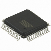
AT32UC3L064-AUT Atmel, AT32UC3L064-AUT Datasheet - Page 617

AT32UC3L064-AUT
Manufacturer Part Number
AT32UC3L064-AUT
Description
MCU AVR32 64KB FLASH 48TQFP
Manufacturer
Atmel
Series
AVR®32 UC3r
Datasheets
1.ATAVRONE-PROBECBL.pdf
(16 pages)
2.AT32UC3L-EK.pdf
(858 pages)
3.AT32UC3L016-D3HT.pdf
(110 pages)
Specifications of AT32UC3L064-AUT
Core Processor
AVR
Core Size
32-Bit
Speed
50MHz
Connectivity
I²C, SPI, UART/USART
Peripherals
Brown-out Detect/Reset, DMA, PWM, WDT
Number Of I /o
36
Program Memory Size
64KB (64K x 8)
Program Memory Type
FLASH
Ram Size
16K x 8
Voltage - Supply (vcc/vdd)
1.62 V ~ 3.6 V
Data Converters
A/D 9x10b
Oscillator Type
Internal
Operating Temperature
-40°C ~ 85°C
Package / Case
48-TQFP, 48-VQFP
Processor Series
AT32UC3x
Core
AVR32
Data Bus Width
32 bit
Data Ram Size
16 KB
Interface Type
SPI/TWI/USART
Maximum Clock Frequency
50 MHz
Number Of Programmable I/os
36
Number Of Timers
7
Maximum Operating Temperature
+ 85 C
Mounting Style
SMD/SMT
3rd Party Development Tools
EWAVR32, EWAVR32-BL
Development Tools By Supplier
AT32UC3L-EK
Minimum Operating Temperature
- 40 C
On-chip Adc
9-ch x 10-bit
Package
48TQFP
Device Core
AVR32
Family Name
AT32
Maximum Speed
50 MHz
Operating Supply Voltage
1.8|3.3 V
Lead Free Status / RoHS Status
Lead free / RoHS Compliant
Eeprom Size
-
Lead Free Status / Rohs Status
Lead free / RoHS Compliant
Available stocks
Company
Part Number
Manufacturer
Quantity
Price
Company:
Part Number:
AT32UC3L064-AUT
Manufacturer:
HONGFA
Quantity:
30 000
Part Number:
AT32UC3L064-AUT
Manufacturer:
MICROCHIP/微芯
Quantity:
20 000
- Current page: 617 of 858
- Download datasheet (13Mb)
26.9.2
Name:
Access Type:
Offset:
Reset Value:
• PENDBC: Pen Detect Debouncing Period
• TSPO: Touch Screen Pin Offset
• APOE: Analog Pin Output Enable
• ACE: Analog Compare Enable
• PENDET: Pen Detect
• TSAMOD: Touch Screen ADC Mode
32099F–11/2010
31
23
15
7
-
-
Period = 2
The Touch Screen Pin Offset field is used to indicate which AD pins are connected to the resistive touch screen film edges. Only
an offset is specified and it is assumed that the resistive touch screen films are connected sequentially from the specified offset
pin and up to and including offset + 3 (4 pins).
0: AD pins are not used to drive VDD in resistive touch screen sequence.
1: AD pins are used to drive VDD in resistive touch screen sequence.
Note: If the selected I/O voltage configuration is incompatible with the Analog-to-Digital converter cell voltage specification, this
bit must stay cleared to avoid damaging the ADC. In this case the ADP pins must be used to drive VDD instead, as described in
Section
case the ADP pins can be ignored.
0: The analog compare functionality is disabled.
1: The analog compare functionality is enabled.
0: The pen detect functionality is disabled.
1: The pen detect functionality is enabled.
0: Touch Screen Mode is disabled.
1: Touch Screen Mode is enabled.
Mode Register
26.7.3. If the I/O and ADC voltages are compatible, the AD pins can be used directly by writing a one to this bit. In this
PENDBC
APOE
30
22
14
6
-
MR
Read/Write
0x04
0x00000000
*T
CLK_ADC
PENDBC
ACE
29
21
13
5
-
PENDET
28
20
12
4
-
TSPO
27
19
11
3
-
-
-
26
18
10
2
-
-
-
AT32UC3L016/32/64
25
17
9
1
-
-
-
TSAMOD
24
16
8
0
-
-
617
Related parts for AT32UC3L064-AUT
Image
Part Number
Description
Manufacturer
Datasheet
Request
R

Part Number:
Description:
KIT DEV/EVAL FOR AT32UC3L0
Manufacturer:
Atmel
Datasheet:

Part Number:
Description:
KIT EVAL AVR32 UC3 MCU
Manufacturer:
Atmel
Datasheet:

Part Number:
Description:
DEV KIT FOR AVR/AVR32
Manufacturer:
Atmel
Datasheet:

Part Number:
Description:
INTERVAL AND WIPE/WASH WIPER CONTROL IC WITH DELAY
Manufacturer:
ATMEL Corporation
Datasheet:

Part Number:
Description:
Low-Voltage Voice-Switched IC for Hands-Free Operation
Manufacturer:
ATMEL Corporation
Datasheet:

Part Number:
Description:
MONOLITHIC INTEGRATED FEATUREPHONE CIRCUIT
Manufacturer:
ATMEL Corporation
Datasheet:

Part Number:
Description:
AM-FM Receiver IC U4255BM-M
Manufacturer:
ATMEL Corporation
Datasheet:

Part Number:
Description:
Monolithic Integrated Feature Phone Circuit
Manufacturer:
ATMEL Corporation
Datasheet:

Part Number:
Description:
Multistandard Video-IF and Quasi Parallel Sound Processing
Manufacturer:
ATMEL Corporation
Datasheet:

Part Number:
Description:
High-performance EE PLD
Manufacturer:
ATMEL Corporation
Datasheet:

Part Number:
Description:
8-bit Flash Microcontroller
Manufacturer:
ATMEL Corporation
Datasheet:

Part Number:
Description:
2-Wire Serial EEPROM
Manufacturer:
ATMEL Corporation
Datasheet:


