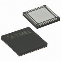
ATMEGA644V-10MU Atmel, ATMEGA644V-10MU Datasheet - Page 166

ATMEGA644V-10MU
Manufacturer Part Number
ATMEGA644V-10MU
Description
IC AVR MCU FLASH 64K 44-QFN
Manufacturer
Atmel
Series
AVR® ATmegar
Specifications of ATMEGA644V-10MU
Core Processor
AVR
Core Size
8-Bit
Speed
10MHz
Connectivity
I²C, SPI, UART/USART
Peripherals
Brown-out Detect/Reset, POR, PWM, WDT
Number Of I /o
32
Program Memory Size
64KB (32K x 16)
Program Memory Type
FLASH
Eeprom Size
2K x 8
Ram Size
4K x 8
Voltage - Supply (vcc/vdd)
1.8 V ~ 5.5 V
Data Converters
A/D 8x10b
Oscillator Type
Internal
Operating Temperature
-40°C ~ 85°C
Package / Case
44-VQFN Exposed Pad
Package
44QFN EP
Device Core
AVR
Family Name
ATmega
Maximum Speed
10 MHz
Operating Supply Voltage
2.5|3.3|5 V
Data Bus Width
8 Bit
Number Of Programmable I/os
32
Interface Type
JTAG/SPI/TWI/USART
On-chip Adc
8-chx10-bit
Number Of Timers
3
Processor Series
ATMEGA64x
Core
AVR8
Data Ram Size
4 KB
Maximum Clock Frequency
20 MHz
Maximum Operating Temperature
+ 85 C
Mounting Style
SMD/SMT
Minimum Operating Temperature
- 40 C
For Use With
ATSTK600-TQFP44 - STK600 SOCKET/ADAPTER 44-TQFPATSTK600 - DEV KIT FOR AVR/AVR32770-1007 - ISP 4PORT ATMEL AVR MCU SPI/JTAGATAVRISP2 - PROGRAMMER AVR IN SYSTEM
Lead Free Status / RoHS Status
Lead free / RoHS Compliant
Available stocks
Company
Part Number
Manufacturer
Quantity
Price
Part Number:
ATMEGA644V-10MU
Manufacturer:
ATMEL/爱特梅尔
Quantity:
20 000
- Current page: 166 of 376
- Download datasheet (8Mb)
17.3.1
166
ATmega644
Internal Clock Generation – The Baud Rate Generator
UCSRnA Register. When using synchronous mode (UMSELn = 1), the Data Direction Register
for the XCKn pin (DDR_XCKn) controls whether the clock source is internal (Master mode) or
external (Slave mode). The XCKn pin is only active when using synchronous mode.
Figure 17-2
Figure 17-2. Clock Generation Logic, Block Diagram
Signal description:
operation.
Internal clock generation is used for the asynchronous and the synchronous master modes of
operation. The description in this section refers to
The USART Baud Rate Register (UBRRn) and the down-counter connected to it function as a
programmable prescaler or baud rate generator. The down-counter, running at system clock
(f
the UBRRLn Register is written. A clock is generated each time the counter reaches zero. This
clock is the baud rate generator clock output (= f
baud rate generator clock output by 2, 8 or 16 depending on mode. The baud rate generator out-
put is used directly by the Receiver’s clock and data recovery units. However, the recovery units
use a state machine that uses 2, 8 or 16 states depending on mode set by the state of the
UMSELn, U2Xn and DDR_XCKn bits.
Table 17-1
ing the UBRRn value for each mode of operation using an internally generated clock source.
Note:
osc
), is loaded with the UBRRn value each time the counter has counted down to zero or when
txclk
rxclk
xcki
xcko
f
OSC
DDR_XCK
1. The baud rate is defined to be the transfer rate in bit per second (bps)
XCK
Pin
contains equations for calculating the baud rate (in bits per second) and for calculat-
shows a block diagram of the clock generation logic.
xcko
xcki
OSC
Transmitter clock (Internal Signal).
Receiver base clock (Internal Signal).
Input from XCK pin (internal Signal). Used for synchronous slave
Clock output to XCK pin (Internal Signal). Used for synchronous master
operation.
XTAL pin frequency (System Clock).
Down-Counter
Prescaling
Register
UBRR
Sync
UBRR+1
fosc
Detector
UCPOL
Edge
/2
Figure
osc
/(UBRRn+1)). The Transmitter divides the
/4
17-2.
/2
DDR_XCK
U2X
0
1
0
1
0
1
1
0
2593N–AVR–07/10
UMSEL
txclk
rxclk
Related parts for ATMEGA644V-10MU
Image
Part Number
Description
Manufacturer
Datasheet
Request
R

Part Number:
Description:
Manufacturer:
Atmel Corporation
Datasheet:

Part Number:
Description:
IC AVR MCU FLASH 64K 44-QFN
Manufacturer:
Atmel
Datasheet:

Part Number:
Description:
IC AVR MCU FLASH 64K 44TQFP
Manufacturer:
Atmel
Datasheet:

Part Number:
Description:
IC AVR MCU FLASH 64K 40DIP
Manufacturer:
Atmel
Datasheet:

Part Number:
Description:
MCU AVR 64K FLASH 20MHZ 44TQFP
Manufacturer:
Atmel
Datasheet:

Part Number:
Description:
MCU AVR 64K FLASH 20MHZ 44QFN
Manufacturer:
Atmel
Datasheet:

Part Number:
Description:
Atmega644 8-bit Avr Microcontroller With 64k Bytes In-system Programmable Flash
Manufacturer:
ATMEL Corporation
Datasheet:

Part Number:
Description:
Manufacturer:
Atmel Corporation
Datasheet:

Part Number:
Description:
Manufacturer:
ATMEL Corporation
Datasheet:

Part Number:
Description:
Manufacturer:
ATMEL Corporation
Datasheet:

Part Number:
Description:
IC AVR MCU 64K 16MHZ 5V 64TQFP
Manufacturer:
Atmel
Datasheet:

Part Number:
Description:
IC AVR MCU 64K 16MHZ 5V 64-QFN
Manufacturer:
Atmel
Datasheet:


