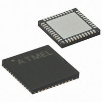
ATMEGA644V-10MU Atmel, ATMEGA644V-10MU Datasheet - Page 255

ATMEGA644V-10MU
Manufacturer Part Number
ATMEGA644V-10MU
Description
IC AVR MCU FLASH 64K 44-QFN
Manufacturer
Atmel
Series
AVR® ATmegar
Specifications of ATMEGA644V-10MU
Core Processor
AVR
Core Size
8-Bit
Speed
10MHz
Connectivity
I²C, SPI, UART/USART
Peripherals
Brown-out Detect/Reset, POR, PWM, WDT
Number Of I /o
32
Program Memory Size
64KB (32K x 16)
Program Memory Type
FLASH
Eeprom Size
2K x 8
Ram Size
4K x 8
Voltage - Supply (vcc/vdd)
1.8 V ~ 5.5 V
Data Converters
A/D 8x10b
Oscillator Type
Internal
Operating Temperature
-40°C ~ 85°C
Package / Case
44-VQFN Exposed Pad
Package
44QFN EP
Device Core
AVR
Family Name
ATmega
Maximum Speed
10 MHz
Operating Supply Voltage
2.5|3.3|5 V
Data Bus Width
8 Bit
Number Of Programmable I/os
32
Interface Type
JTAG/SPI/TWI/USART
On-chip Adc
8-chx10-bit
Number Of Timers
3
Processor Series
ATMEGA64x
Core
AVR8
Data Ram Size
4 KB
Maximum Clock Frequency
20 MHz
Maximum Operating Temperature
+ 85 C
Mounting Style
SMD/SMT
Minimum Operating Temperature
- 40 C
For Use With
ATSTK600-TQFP44 - STK600 SOCKET/ADAPTER 44-TQFPATSTK600 - DEV KIT FOR AVR/AVR32770-1007 - ISP 4PORT ATMEL AVR MCU SPI/JTAGATAVRISP2 - PROGRAMMER AVR IN SYSTEM
Lead Free Status / RoHS Status
Lead free / RoHS Compliant
Available stocks
Company
Part Number
Manufacturer
Quantity
Price
Part Number:
ATMEGA644V-10MU
Manufacturer:
ATMEL/爱特梅尔
Quantity:
20 000
- Current page: 255 of 376
- Download datasheet (8Mb)
22.3
2593N–AVR–07/10
TAP Controller
Figure 22-2. TAP Controller State Diagram
The TAP controller is a 16-state finite state machine that controls the operation of the Boundary-
scan circuitry, JTAG programming circuitry, or On-chip Debug system. The state transitions
depicted in
transition) at the time of the rising edge at TCK. The initial state after a Power-on Reset is Test-
Logic-Reset.
As a definition in this document, the LSB is shifted in and out first for all Shift Registers.
Assuming Run-Test/Idle is the present state, a typical scenario for using the JTAG interface is:
• At the TMS input, apply the sequence 1, 1, 0, 0 at the rising edges of TCK to enter the Shift
Instruction Register – Shift-IR state. While in this state, shift the four bits of the JTAG
instructions into the JTAG Instruction Register from the TDI input at the rising edge of TCK.
The TMS input must be held low during input of the 3 LSBs in order to remain in the Shift-IR
state. The MSB of the instruction is shifted in when this state is left by setting TMS high. While
the instruction is shifted in from the TDI pin, the captured IR-state 0x01 is shifted out on the
TDO pin. The JTAG Instruction selects a particular Data Register as path between TDI and
TDO and controls the circuitry surrounding the selected Data Register.
1
0
Figure 22-2
Test-Logic-Reset
Run-Test/Idle
0
depend on the signal present on TMS (shown adjacent to each state
1
1
0
Select-DR Scan
Capture-DR
Update-DR
Pause-DR
Exit1-DR
Exit2-DR
Shift-DR
1
0
0
1
0
1
1
0
1
1
0
0
1
0
Select-IR Scan
Capture-IR
Update-IR
Pause-IR
Exit1-IR
Exit2-IR
Shift-IR
1
ATmega644
0
0
1
0
1
1
0
1
1
0
0
255
Related parts for ATMEGA644V-10MU
Image
Part Number
Description
Manufacturer
Datasheet
Request
R

Part Number:
Description:
Manufacturer:
Atmel Corporation
Datasheet:

Part Number:
Description:
IC AVR MCU FLASH 64K 44-QFN
Manufacturer:
Atmel
Datasheet:

Part Number:
Description:
IC AVR MCU FLASH 64K 44TQFP
Manufacturer:
Atmel
Datasheet:

Part Number:
Description:
IC AVR MCU FLASH 64K 40DIP
Manufacturer:
Atmel
Datasheet:

Part Number:
Description:
MCU AVR 64K FLASH 20MHZ 44TQFP
Manufacturer:
Atmel
Datasheet:

Part Number:
Description:
MCU AVR 64K FLASH 20MHZ 44QFN
Manufacturer:
Atmel
Datasheet:

Part Number:
Description:
Atmega644 8-bit Avr Microcontroller With 64k Bytes In-system Programmable Flash
Manufacturer:
ATMEL Corporation
Datasheet:

Part Number:
Description:
Manufacturer:
Atmel Corporation
Datasheet:

Part Number:
Description:
Manufacturer:
ATMEL Corporation
Datasheet:

Part Number:
Description:
Manufacturer:
ATMEL Corporation
Datasheet:

Part Number:
Description:
IC AVR MCU 64K 16MHZ 5V 64TQFP
Manufacturer:
Atmel
Datasheet:

Part Number:
Description:
IC AVR MCU 64K 16MHZ 5V 64-QFN
Manufacturer:
Atmel
Datasheet:


