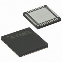
ATMEGA644V-10MU Atmel, ATMEGA644V-10MU Datasheet - Page 75

ATMEGA644V-10MU
Manufacturer Part Number
ATMEGA644V-10MU
Description
IC AVR MCU FLASH 64K 44-QFN
Manufacturer
Atmel
Series
AVR® ATmegar
Specifications of ATMEGA644V-10MU
Core Processor
AVR
Core Size
8-Bit
Speed
10MHz
Connectivity
I²C, SPI, UART/USART
Peripherals
Brown-out Detect/Reset, POR, PWM, WDT
Number Of I /o
32
Program Memory Size
64KB (32K x 16)
Program Memory Type
FLASH
Eeprom Size
2K x 8
Ram Size
4K x 8
Voltage - Supply (vcc/vdd)
1.8 V ~ 5.5 V
Data Converters
A/D 8x10b
Oscillator Type
Internal
Operating Temperature
-40°C ~ 85°C
Package / Case
44-VQFN Exposed Pad
Package
44QFN EP
Device Core
AVR
Family Name
ATmega
Maximum Speed
10 MHz
Operating Supply Voltage
2.5|3.3|5 V
Data Bus Width
8 Bit
Number Of Programmable I/os
32
Interface Type
JTAG/SPI/TWI/USART
On-chip Adc
8-chx10-bit
Number Of Timers
3
Processor Series
ATMEGA64x
Core
AVR8
Data Ram Size
4 KB
Maximum Clock Frequency
20 MHz
Maximum Operating Temperature
+ 85 C
Mounting Style
SMD/SMT
Minimum Operating Temperature
- 40 C
For Use With
ATSTK600-TQFP44 - STK600 SOCKET/ADAPTER 44-TQFPATSTK600 - DEV KIT FOR AVR/AVR32770-1007 - ISP 4PORT ATMEL AVR MCU SPI/JTAGATAVRISP2 - PROGRAMMER AVR IN SYSTEM
Lead Free Status / RoHS Status
Lead free / RoHS Compliant
Available stocks
Company
Part Number
Manufacturer
Quantity
Price
Part Number:
ATMEGA644V-10MU
Manufacturer:
ATMEL/爱特梅尔
Quantity:
20 000
- Current page: 75 of 376
- Download datasheet (8Mb)
12.3.2
2593N–AVR–07/10
Alternate Functions of Port B
The Port B pins with alternate functions are shown in
Table 12-6.
The alternate pin configuration is as follows:
• SCK/PCINT15 – Port B, Bit 7
SCK: Master Clock output, Slave Clock input pin for SPI channel. When the SPI is enabled as a
slave, this pin is configured as an input regardless of the setting of DDB7. When the SPI0 is
enabled as a master, the data direction of this pin is controlled by DDB7. When the pin is forced
to be an input, the pull-up can still be controlled by the PORTB7 bit.
PCINT15, Pin Change Interrupt source 15: The PB7 pin can serve as an external interrupt
source.
• MISO/PCINT14 – Port B, Bit 6
MISO: Master Data input, Slave Data output pin for SPI channel. When the SPI is enabled as a
master, this pin is configured as an input regardless of the setting of DDB6. When the SPI is
enabled as a slave, the data direction of this pin is controlled by DDB6. When the pin is forced to
be an input, the pull-up can still be controlled by the PORTB6 bit.
PCINT14, Pin Change Interrupt source 14: The PB6 pin can serve as an external interrupt
source.
Port Pin
PB7
PB6
PB5
PB4
PB3
PB2
PB1
PB0
Alternate Functions
SCK (SPI Bus Master clock input)
PCINT15 (Pin Change Interrupt 15)
MISO (SPI Bus Master Input/Slave Output)
PCINT14 (Pin Change Interrupt 14)
MOSI (SPI Bus Master Output/Slave Input)
PCINT13 (Pin Change Interrupt 13)
SS (SPI Slave Select input)
OC0B (Timer/Conter 0 Output Compare Match B Output)
PCINT12 (Pin Change Interrupt 12)
AIN1 (Analog Comparator Negative Input)
OC0A (Timer/Conter 0 Output Compare Match A Output)
PCINT11 (Pin Change Interrupt 11)
AIN0 (Analog Comparator Positive Input)
INT2 (External Interrupt 2 Input)
PCINT10 (Pin Change Interrupt 10)
T1 (Timer/Counter 1 External Counter Input)
CLKO (Divided System Clock Output)
PCINT9 (Pin Change Interrupt 9)
T0 (Timer/Counter 0 External Counter Input)
XCK0 (USART0 External Clock Input/Output)
PCINT8 (Pin Change Interrupt 8)
Port B Pins Alternate Functions
Table
12-6.
ATmega644
75
Related parts for ATMEGA644V-10MU
Image
Part Number
Description
Manufacturer
Datasheet
Request
R

Part Number:
Description:
Manufacturer:
Atmel Corporation
Datasheet:

Part Number:
Description:
IC AVR MCU FLASH 64K 44-QFN
Manufacturer:
Atmel
Datasheet:

Part Number:
Description:
IC AVR MCU FLASH 64K 44TQFP
Manufacturer:
Atmel
Datasheet:

Part Number:
Description:
IC AVR MCU FLASH 64K 40DIP
Manufacturer:
Atmel
Datasheet:

Part Number:
Description:
MCU AVR 64K FLASH 20MHZ 44TQFP
Manufacturer:
Atmel
Datasheet:

Part Number:
Description:
MCU AVR 64K FLASH 20MHZ 44QFN
Manufacturer:
Atmel
Datasheet:

Part Number:
Description:
Atmega644 8-bit Avr Microcontroller With 64k Bytes In-system Programmable Flash
Manufacturer:
ATMEL Corporation
Datasheet:

Part Number:
Description:
Manufacturer:
Atmel Corporation
Datasheet:

Part Number:
Description:
Manufacturer:
ATMEL Corporation
Datasheet:

Part Number:
Description:
Manufacturer:
ATMEL Corporation
Datasheet:

Part Number:
Description:
IC AVR MCU 64K 16MHZ 5V 64TQFP
Manufacturer:
Atmel
Datasheet:

Part Number:
Description:
IC AVR MCU 64K 16MHZ 5V 64-QFN
Manufacturer:
Atmel
Datasheet:


