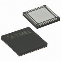
ATMEGA644V-10MU Atmel, ATMEGA644V-10MU Datasheet - Page 93

ATMEGA644V-10MU
Manufacturer Part Number
ATMEGA644V-10MU
Description
IC AVR MCU FLASH 64K 44-QFN
Manufacturer
Atmel
Series
AVR® ATmegar
Specifications of ATMEGA644V-10MU
Core Processor
AVR
Core Size
8-Bit
Speed
10MHz
Connectivity
I²C, SPI, UART/USART
Peripherals
Brown-out Detect/Reset, POR, PWM, WDT
Number Of I /o
32
Program Memory Size
64KB (32K x 16)
Program Memory Type
FLASH
Eeprom Size
2K x 8
Ram Size
4K x 8
Voltage - Supply (vcc/vdd)
1.8 V ~ 5.5 V
Data Converters
A/D 8x10b
Oscillator Type
Internal
Operating Temperature
-40°C ~ 85°C
Package / Case
44-VQFN Exposed Pad
Package
44QFN EP
Device Core
AVR
Family Name
ATmega
Maximum Speed
10 MHz
Operating Supply Voltage
2.5|3.3|5 V
Data Bus Width
8 Bit
Number Of Programmable I/os
32
Interface Type
JTAG/SPI/TWI/USART
On-chip Adc
8-chx10-bit
Number Of Timers
3
Processor Series
ATMEGA64x
Core
AVR8
Data Ram Size
4 KB
Maximum Clock Frequency
20 MHz
Maximum Operating Temperature
+ 85 C
Mounting Style
SMD/SMT
Minimum Operating Temperature
- 40 C
For Use With
ATSTK600-TQFP44 - STK600 SOCKET/ADAPTER 44-TQFPATSTK600 - DEV KIT FOR AVR/AVR32770-1007 - ISP 4PORT ATMEL AVR MCU SPI/JTAGATAVRISP2 - PROGRAMMER AVR IN SYSTEM
Lead Free Status / RoHS Status
Lead free / RoHS Compliant
Available stocks
Company
Part Number
Manufacturer
Quantity
Price
Part Number:
ATMEGA644V-10MU
Manufacturer:
ATMEL/爱特梅尔
Quantity:
20 000
- Current page: 93 of 376
- Download datasheet (8Mb)
2593N–AVR–07/10
PWM mode is shown in
togram for illustrating the single-slope operation. The diagram includes non-inverted and
inverted PWM outputs. The small horizontal line marks on the TCNT0 slopes represent Com-
pare Matches between OCR0x and TCNT0.
Figure 13-6. Fast PWM Mode, Timing Diagram
The Timer/Counter Overflow Flag (TOV0) is set each time the counter reaches TOP. If the inter-
rupt is enabled, the interrupt handler routine can be used for updating the compare value.
In fast PWM mode, the compare unit allows generation of PWM waveforms on the OC0x pins.
Setting the COM0x1:0 bits to two will produce a non-inverted PWM and an inverted PWM output
can be generated by setting the COM0x1:0 to three: Setting the COM0A1:0 bits to one allows
the OC0A pin to toggle on Compare Matches if the WGM02 bit is set. This option is not available
for the OC0B pin (See
port pin if the data direction for the port pin is set as output. The PWM waveform is generated by
setting (or clearing) the OC0x Register at the Compare Match between OCR0x and TCNT0, and
clearing (or setting) the OC0x Register at the timer clock cycle the counter is cleared (changes
from TOP to BOTTOM).
The PWM frequency for the output can be calculated by the following equation:
The N variable represents the prescale factor (1, 8, 64, 256, or 1024).
The extreme values for the OCR0A Register represents special cases when generating a PWM
waveform output in the fast PWM mode. If the OCR0A is set equal to BOTTOM, the output will
be a narrow spike for each MAX+1 timer clock cycle. Setting the OCR0A equal to MAX will result
in a constantly high or low output (depending on the polarity of the output set by the COM0A1:0
bits.)
A frequency (with 50% duty cycle) waveform output in fast PWM mode can be achieved by set-
ting OC0x to toggle its logical level on each Compare Match (COM0x1:0 = 1). The waveform
generated will have a maximum frequency of f
TCNTn
OCnx
OCnx
Period
1
Table 13-3 on page
Figure
2
13-6. The TCNT0 value is in the timing diagram shown as a his-
3
f
OCnxPWM
4
97). The actual OC0x value will only be visible on the
OC0
5
=
----------------- -
N 256
f
= f
clk_I/O
⋅
clk_I/O
6
/2 when OCR0A is set to zero. This
7
ATmega644
OCRnx Interrupt Flag Set
OCRnx Update and
TOVn Interrupt Flag Set
(COMnx1:0 = 2)
(COMnx1:0 = 3)
93
Related parts for ATMEGA644V-10MU
Image
Part Number
Description
Manufacturer
Datasheet
Request
R

Part Number:
Description:
Manufacturer:
Atmel Corporation
Datasheet:

Part Number:
Description:
IC AVR MCU FLASH 64K 44-QFN
Manufacturer:
Atmel
Datasheet:

Part Number:
Description:
IC AVR MCU FLASH 64K 44TQFP
Manufacturer:
Atmel
Datasheet:

Part Number:
Description:
IC AVR MCU FLASH 64K 40DIP
Manufacturer:
Atmel
Datasheet:

Part Number:
Description:
MCU AVR 64K FLASH 20MHZ 44TQFP
Manufacturer:
Atmel
Datasheet:

Part Number:
Description:
MCU AVR 64K FLASH 20MHZ 44QFN
Manufacturer:
Atmel
Datasheet:

Part Number:
Description:
Atmega644 8-bit Avr Microcontroller With 64k Bytes In-system Programmable Flash
Manufacturer:
ATMEL Corporation
Datasheet:

Part Number:
Description:
Manufacturer:
Atmel Corporation
Datasheet:

Part Number:
Description:
Manufacturer:
ATMEL Corporation
Datasheet:

Part Number:
Description:
Manufacturer:
ATMEL Corporation
Datasheet:

Part Number:
Description:
IC AVR MCU 64K 16MHZ 5V 64TQFP
Manufacturer:
Atmel
Datasheet:

Part Number:
Description:
IC AVR MCU 64K 16MHZ 5V 64-QFN
Manufacturer:
Atmel
Datasheet:


