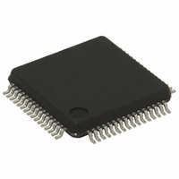
STR711FR2T6 STMicroelectronics, STR711FR2T6 Datasheet - Page 60

STR711FR2T6
Manufacturer Part Number
STR711FR2T6
Description
IC MCU ARM7 TDMI 256K 64-LQFP
Manufacturer
STMicroelectronics
Series
STR7r
Datasheet
1.RLINK-ST.pdf
(78 pages)
Specifications of STR711FR2T6
Core Processor
ARM7
Core Size
32-Bit
Speed
66MHz
Connectivity
HDLC, I²C, SmartCard, SPI, UART/USART, USB
Peripherals
PWM, WDT
Number Of I /o
30
Program Memory Size
256KB (256K x 8 + 16K)
Program Memory Type
FLASH
Ram Size
64K x 8
Voltage - Supply (vcc/vdd)
3 V ~ 3.6 V
Data Converters
A/D 4x12b
Oscillator Type
Internal
Operating Temperature
-40°C ~ 85°C
Package / Case
64-LQFP
Processor Series
STR711x
Core
ARM7TDMI
Data Bus Width
32 bit
Data Ram Size
64 KB
Interface Type
CAN/EMI/USB
Maximum Clock Frequency
66 MHz
Number Of Programmable I/os
30
Number Of Timers
4
Operating Supply Voltage
3 V to 3.6 V
Maximum Operating Temperature
+ 85 C
Mounting Style
SMD/SMT
3rd Party Development Tools
EWARM, EWARM-BL, MCBSTR7, KSK-STR711-PL, MDK-ARM, RL-ARM, ULINK2
Development Tools By Supplier
STR710-SK/HIT, STR711-SK/IAR, STR712-SK/IAR, STR71X-SK/RAIS, STX-PRO/RAIS, STX-RLINK, STR79-RVDK/CPP, STR79-RVDK, STR79-RVDK/UPG
Minimum Operating Temperature
- 40 C
On-chip Adc
4-ch x 12-bit
For Use With
MCBSTR7UME - MCBSTR7 + ULINK-ME DEV KITMCBSTR7 - BOARD EVAL STM STR71X SERIES497-5046 - KIT TOOL FOR ST7/UPSD/STR7 MCU497-4550 - KIT IAR STARTER STR711/STR712
Lead Free Status / RoHS Status
Lead free / RoHS Compliant
Eeprom Size
-
Lead Free Status / Rohs Status
Lead free / RoHS Compliant
Other names
497-4513
Available stocks
Company
Part Number
Manufacturer
Quantity
Price
Company:
Part Number:
STR711FR2T6
Manufacturer:
ST
Quantity:
74
Company:
Part Number:
STR711FR2T6
Manufacturer:
STMicroelect
Quantity:
749
Company:
Part Number:
STR711FR2T6
Manufacturer:
STMicroelectronics
Quantity:
10 000
Part Number:
STR711FR2T6
Manufacturer:
ST
Quantity:
20 000
Electrical parameters
4.3.8
Note:
60/78
Figure 31. Write cycle timing: 16-bit write on 8-bit memory
Figure 32. Write cycle timing: 32-bit write on 8-bit memory
I
Subject to general operating conditions for V
The STR7 I
protocol described in the following table with the restriction mentioned below:
Restriction: The I/O pins which SDA and SCL are mapped to are not “True” Open-Drain:
when configured as open-drain, the PMOS connected between the I/O pin and V
disabled, but it is still present. Also, there is a protection diode between the I/O pin and V
Consequently, when using this I
the STR7X while some another I
STR7X will be powered by the protection diode.
Refer to I/O port characteristics for more details on the input/output alternate function
characteristics (SDA and SCL).
2
RDn
CSn.x
WEn.x
D[7:0]
(Output)
A[23:0]
C - inter IC control interface
RDn
CSn.x
WEn.x
D[7:0]
(Output)
A[23:0]
See
2
C interface meets the requirements of the Standard I
Table 35
t
WAS
address
t
WAS
for write timing data.
t
WP
Data Output
t
WDS1
t
WAH
address
t
WAT
t
t
WWT
WDH
2
t
2
WP
C in a multi-master network, it is not possible to power off
C master node remains powered on: otherwise, the
Data Output
t
WDS1
address
t
WAH
t
WP
Data Output
t
WDS2
t
WAT
t
WAH
t
t
WWT
WDH
t
WAT
33
t
t
WWT
WDH
, f
PCLK1
address
address
t
t
WP
WP
Data Output
Data Output
t
WDS2
, and T
t
WDS2
t
WAH
t
WAH
t
WAT
t
t
WWT
WDH
A
t
t
WCR
WDH
unless otherwise specified.
address
2
t
WP
C communications
Data Output
t
WDS2
t
WAH
t
t
WCR
WDH
33
STR71xF
is
33
.


