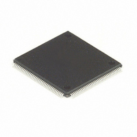
MC68HC16Z1CPV25 Freescale Semiconductor, MC68HC16Z1CPV25 Datasheet - Page 138

MC68HC16Z1CPV25
Manufacturer Part Number
MC68HC16Z1CPV25
Description
IC MPU 1K RAM 25MHZ 144-LQFP
Manufacturer
Freescale Semiconductor
Series
HC16r
Datasheet
1.MC68HC16Z1VEH16.pdf
(500 pages)
Specifications of MC68HC16Z1CPV25
Core Processor
CPU16
Core Size
16-Bit
Speed
25MHz
Connectivity
EBI/EMI, SCI, SPI
Peripherals
POR, PWM, WDT
Number Of I /o
16
Program Memory Type
ROMless
Ram Size
1K x 8
Voltage - Supply (vcc/vdd)
2.7 V ~ 5.5 V
Data Converters
A/D 8x10b
Oscillator Type
Internal
Operating Temperature
-40°C ~ 85°C
Package / Case
144-LQFP
Lead Free Status / RoHS Status
Contains lead / RoHS non-compliant
Eeprom Size
-
Program Memory Size
-
Other names
Q1141110
Available stocks
Company
Part Number
Manufacturer
Quantity
Price
Company:
Part Number:
MC68HC16Z1CPV25
Manufacturer:
MOT
Quantity:
5 510
Company:
Part Number:
MC68HC16Z1CPV25
Manufacturer:
SIEMENS
Quantity:
5 510
Company:
Part Number:
MC68HC16Z1CPV25
Manufacturer:
FREESCAL
Quantity:
624
Company:
Part Number:
MC68HC16Z1CPV25
Manufacturer:
Freescale Semiconductor
Quantity:
10 000
- Current page: 138 of 500
- Download datasheet (6Mb)
5.5.1.5 Read/Write Signal
5.5.1.6 Size Signals
5.5.1.7 Function Codes
5.5.1.8 Data Size Acknowledge Signals
5-32
The read/write signal (R/W) determines the direction of the transfer during a bus cycle.
This signal changes state, when required, at the beginning of a bus cycle, and is valid
while AS is asserted. R/W only transitions when a write cycle is preceded by a read
cycle or vice versa. The signal may remain low for two consecutive write cycles.
Size signals (SIZ[1:0]) indicate the number of bytes remaining to be transferred during
an operand cycle. They are valid while AS is asserted.
SIZ1 encoding.
The CPU generates function code signals (FC[2:0]) to indicate the type of activity oc-
curring on the data or address bus. These signals can be considered address exten-
sions that can be externally decoded to determine which of eight external address
spaces is accessed during a bus cycle.
Because the CPU16 always operates in supervisor mode (FC2 = 1), address spaces
0 to 3 are not used. Address space 7 is designated CPU space. CPU space is used
for control information not normally associated with read or write bus cycles. Function
codes are valid while AS is asserted.
During normal bus transfers, external devices assert the data size acknowledge sig-
nals (DSACK[1:0]) to indicate port width to the MCU. During a read cycle, these sig-
nals tell the MCU to terminate the bus cycle and to latch data. During a write cycle, the
signals indicate that an external device has successfully stored data and that the cycle
can terminate. DSACK[1:0] can also be supplied internally by chip-select logic. Refer
to
5.9 Chip-Selects
FC2
1
1
1
1
Freescale Semiconductor, Inc.
for more information.
Table 5-14 Address Space Encoding
For More Information On This Product,
Table 5-13 Size Signal Encoding
SIZ1
0
1
1
0
SYSTEM INTEGRATION MODULE
Go to: www.freescale.com
FC1
0
0
1
1
Table 5-14
SIZ0
1
0
1
0
FC0
0
1
0
1
shows address space encoding.
Transfer Size
Long Word
3 Byte
Word
Byte
Table 5-13
Address Space
Program space
Data space
CPU space
Reserved
M68HC16 Z SERIES
shows SIZ0 and
USER’S MANUAL
Related parts for MC68HC16Z1CPV25
Image
Part Number
Description
Manufacturer
Datasheet
Request
R
Part Number:
Description:
Manufacturer:
Freescale Semiconductor, Inc
Datasheet:
Part Number:
Description:
Manufacturer:
Freescale Semiconductor, Inc
Datasheet:
Part Number:
Description:
Manufacturer:
Freescale Semiconductor, Inc
Datasheet:
Part Number:
Description:
Manufacturer:
Freescale Semiconductor, Inc
Datasheet:
Part Number:
Description:
Manufacturer:
Freescale Semiconductor, Inc
Datasheet:
Part Number:
Description:
Manufacturer:
Freescale Semiconductor, Inc
Datasheet:
Part Number:
Description:
Manufacturer:
Freescale Semiconductor, Inc
Datasheet:
Part Number:
Description:
Manufacturer:
Freescale Semiconductor, Inc
Datasheet:
Part Number:
Description:
Manufacturer:
Freescale Semiconductor, Inc
Datasheet:
Part Number:
Description:
Manufacturer:
Freescale Semiconductor, Inc
Datasheet:
Part Number:
Description:
Manufacturer:
Freescale Semiconductor, Inc
Datasheet:
Part Number:
Description:
Manufacturer:
Freescale Semiconductor, Inc
Datasheet:
Part Number:
Description:
Manufacturer:
Freescale Semiconductor, Inc
Datasheet:
Part Number:
Description:
Manufacturer:
Freescale Semiconductor, Inc
Datasheet:
Part Number:
Description:
Manufacturer:
Freescale Semiconductor, Inc
Datasheet:


