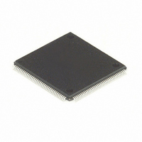
MC68HC16Z1CPV25 Freescale Semiconductor, MC68HC16Z1CPV25 Datasheet - Page 238

MC68HC16Z1CPV25
Manufacturer Part Number
MC68HC16Z1CPV25
Description
IC MPU 1K RAM 25MHZ 144-LQFP
Manufacturer
Freescale Semiconductor
Series
HC16r
Datasheet
1.MC68HC16Z1VEH16.pdf
(500 pages)
Specifications of MC68HC16Z1CPV25
Core Processor
CPU16
Core Size
16-Bit
Speed
25MHz
Connectivity
EBI/EMI, SCI, SPI
Peripherals
POR, PWM, WDT
Number Of I /o
16
Program Memory Type
ROMless
Ram Size
1K x 8
Voltage - Supply (vcc/vdd)
2.7 V ~ 5.5 V
Data Converters
A/D 8x10b
Oscillator Type
Internal
Operating Temperature
-40°C ~ 85°C
Package / Case
144-LQFP
Lead Free Status / RoHS Status
Contains lead / RoHS non-compliant
Eeprom Size
-
Program Memory Size
-
Other names
Q1141110
Available stocks
Company
Part Number
Manufacturer
Quantity
Price
Company:
Part Number:
MC68HC16Z1CPV25
Manufacturer:
MOT
Quantity:
5 510
Company:
Part Number:
MC68HC16Z1CPV25
Manufacturer:
SIEMENS
Quantity:
5 510
Company:
Part Number:
MC68HC16Z1CPV25
Manufacturer:
FREESCAL
Quantity:
624
Company:
Part Number:
MC68HC16Z1CPV25
Manufacturer:
Freescale Semiconductor
Quantity:
10 000
- Current page: 238 of 500
- Download datasheet (6Mb)
9.4.3.6 Receiver Operation
9-28
If TE remains set, after all pending idle, data and break frames are shifted out, TDRE
and TC are set and TXD is held at logic level one (mark).
When TE is cleared, the transmitter is disabled after all pending idle, data, and break
frames are transmitted. The TC flag is set, and control of the TXD pin reverts to
PQSPAR and DDRQS. Buffered data is not transmitted after TE is cleared. To avoid
losing data in the buffer, do not clear TE until TDRE is set.
Some serial communication systems require a mark on the TXD pin even when the
transmitter is disabled. Configure the TXD pin as an output, then write a one to PQS7.
When the transmitter releases control of the TXD pin, it will revert to driving a logic one
output.
To insert a delimiter between two messages, to place non-listening receivers in wake-
up mode between transmissions, or to signal a retransmission by forcing an idle line,
clear and then set TE before data in the serial shifter has shifted out. The transmitter
finishes the transmission, then sends a preamble. After the preamble is transmitted, if
TDRE is set, the transmitter will mark idle. Otherwise, normal transmission of the next
sequence will begin.
Both TDRE and TC have associated interrupts. The interrupts are enabled by the
transmit interrupt enable (TIE) and transmission complete interrupt enable (TCIE) bits
in SCCR1. Service routines can load the last byte of data in a sequence into SCDR,
then terminate the transmission when a TDRE interrupt occurs.
The RE bit in SCCR1 enables (RE = 1) and disables (RE = 0) the receiver. The receiv-
er contains a receive serial shifter and a parallel receive data register (RDR) located
in the SCI data register (SCDR). The serial shifter cannot be directly accessed by the
CPU16. The receiver is double-buffered, allowing data to be held in RDR while other
data is shifted in.
Receiver bit processor logic drives a state machine that determines the logic level for
each bit-time. This state machine controls when the bit processor logic is to sample
the RXD pin and also controls when data is to be passed to the receive serial shifter.
A receive time clock is used to control sampling and synchronization. Data is shifted
into the receive serial shifter according to the most recent synchronization of the re-
ceive time clock with the incoming data stream. From this point on, data movement is
synchronized with the MCU system clock. Operation of the receiver state machine is
detailed in the QSM Reference Manual (QSMRM/AD).
The number of bits shifted in by the receiver depends on the serial format. However,
all frames must end with at least one stop bit. When the stop bit is received, the frame
is considered to be complete, and the received data in the serial shifter is transferred
to RDR. The receiver data register flag (RDRF) is set when the data is transferred.
Noise errors, parity errors, and framing errors can be detected while a data stream is
being received. Although error conditions are detected as bits are received, the noise
flag (NF), the parity flag (PF), and the framing error (FE) flag in SCSR are not set until
data is transferred from the serial shifter to RDR.
Freescale Semiconductor, Inc.
For More Information On This Product,
QUEUED SERIAL MODULE
Go to: www.freescale.com
M68HC16 Z SERIES
USER’S MANUAL
Related parts for MC68HC16Z1CPV25
Image
Part Number
Description
Manufacturer
Datasheet
Request
R
Part Number:
Description:
Manufacturer:
Freescale Semiconductor, Inc
Datasheet:
Part Number:
Description:
Manufacturer:
Freescale Semiconductor, Inc
Datasheet:
Part Number:
Description:
Manufacturer:
Freescale Semiconductor, Inc
Datasheet:
Part Number:
Description:
Manufacturer:
Freescale Semiconductor, Inc
Datasheet:
Part Number:
Description:
Manufacturer:
Freescale Semiconductor, Inc
Datasheet:
Part Number:
Description:
Manufacturer:
Freescale Semiconductor, Inc
Datasheet:
Part Number:
Description:
Manufacturer:
Freescale Semiconductor, Inc
Datasheet:
Part Number:
Description:
Manufacturer:
Freescale Semiconductor, Inc
Datasheet:
Part Number:
Description:
Manufacturer:
Freescale Semiconductor, Inc
Datasheet:
Part Number:
Description:
Manufacturer:
Freescale Semiconductor, Inc
Datasheet:
Part Number:
Description:
Manufacturer:
Freescale Semiconductor, Inc
Datasheet:
Part Number:
Description:
Manufacturer:
Freescale Semiconductor, Inc
Datasheet:
Part Number:
Description:
Manufacturer:
Freescale Semiconductor, Inc
Datasheet:
Part Number:
Description:
Manufacturer:
Freescale Semiconductor, Inc
Datasheet:
Part Number:
Description:
Manufacturer:
Freescale Semiconductor, Inc
Datasheet:


