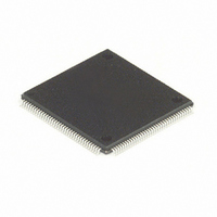
MC68HC16Z1CPV25 Freescale Semiconductor, MC68HC16Z1CPV25 Datasheet - Page 392

MC68HC16Z1CPV25
Manufacturer Part Number
MC68HC16Z1CPV25
Description
IC MPU 1K RAM 25MHZ 144-LQFP
Manufacturer
Freescale Semiconductor
Series
HC16r
Datasheet
1.MC68HC16Z1VEH16.pdf
(500 pages)
Specifications of MC68HC16Z1CPV25
Core Processor
CPU16
Core Size
16-Bit
Speed
25MHz
Connectivity
EBI/EMI, SCI, SPI
Peripherals
POR, PWM, WDT
Number Of I /o
16
Program Memory Type
ROMless
Ram Size
1K x 8
Voltage - Supply (vcc/vdd)
2.7 V ~ 5.5 V
Data Converters
A/D 8x10b
Oscillator Type
Internal
Operating Temperature
-40°C ~ 85°C
Package / Case
144-LQFP
Lead Free Status / RoHS Status
Contains lead / RoHS non-compliant
Eeprom Size
-
Program Memory Size
-
Other names
Q1141110
Available stocks
Company
Part Number
Manufacturer
Quantity
Price
Company:
Part Number:
MC68HC16Z1CPV25
Manufacturer:
MOT
Quantity:
5 510
Company:
Part Number:
MC68HC16Z1CPV25
Manufacturer:
SIEMENS
Quantity:
5 510
Company:
Part Number:
MC68HC16Z1CPV25
Manufacturer:
FREESCAL
Quantity:
624
Company:
Part Number:
MC68HC16Z1CPV25
Manufacturer:
Freescale Semiconductor
Quantity:
10 000
- Current page: 392 of 500
- Download datasheet (6Mb)
ADDR[23:11] — Base Address
BLKSZ[2:0] — Block Size Field
D.2.20 Chip-Select Option Register Boot
CSORBT — Chip-Select Option Register Boot
D.2.21 Chip-Select Option Registers
CSOR[0:10] — Chip-Select Option Registers
D-18
MODE
MODE
15
15
0
0
RESET:
RESET:
Each chip-select pin has an associated base address register. A base address is the
lowest address in the block of addresses enabled by a chip select. CSBARBT contains
the base address for selection of a boot memory device. Bit and field definitions for
CSBARBT and CSBAR[0:10] are the same, but reset block sizes differ. These regis-
ters may be read or written at any time.
This field sets the starting address of a particular chip-select’s address space. The ad-
dress compare logic uses only the most significant bits to match an address within a
block. The value of the base address must be an integer multiple of the block size.
Base address register diagrams show how base register bits correspond to address
lines.
This field determines the size of the block that is enabled by the chip-select.
Table D-12
14
14
1
0
BYTE[1:0]
BYTE[1:0]
13
13
1
0
shows bit encoding for the base address registers block size field.
12
12
1
0
R/W[1:0]
R/W[1:0]
NOTES:
Table D-12 Block Size Field Bit Encoding
BLKSZ[2:0]
Freescale Semiconductor, Inc.
1. ADDR[23:20] are the same logic level as ADDR19 during
11
11
1
0
normal operation.
For More Information On This Product,
000
001
010
011
100
101
110
111
STRB
STRB
10
10
0
0
Go to: www.freescale.com
REGISTER SUMMARY
Block Size
128 Kbytes
256 Kbytes
512 Kbytes
512 Kbytes
9
1
9
0
16 Kbytes
64 Kbytes
2 Kbytes
8 Kbytes
DSACK[3:0]
DSACK[3:0]
8
1
8
0
Address Lines Compared
7
0
7
0
ADDR[23:11]
ADDR[23:13]
ADDR[23:14]
ADDR[23:16]
ADDR[23:17]
ADDR[23:18]
ADDR[23:19]
ADDR[23:20]
6
1
6
0
SPACE[1:0]
SPACE[1:0]
5
1
5
0
4
1
4
0
1
$YFFA4E–YFFA76
3
0
3
0
M68HC16 Z SERIES
IPL[2:0]
IPL[2:0]
USER’S MANUAL
2
0
2
0
$YFFA4A
1
0
1
0
AVEC
AVEC
0
0
0
0
Related parts for MC68HC16Z1CPV25
Image
Part Number
Description
Manufacturer
Datasheet
Request
R
Part Number:
Description:
Manufacturer:
Freescale Semiconductor, Inc
Datasheet:
Part Number:
Description:
Manufacturer:
Freescale Semiconductor, Inc
Datasheet:
Part Number:
Description:
Manufacturer:
Freescale Semiconductor, Inc
Datasheet:
Part Number:
Description:
Manufacturer:
Freescale Semiconductor, Inc
Datasheet:
Part Number:
Description:
Manufacturer:
Freescale Semiconductor, Inc
Datasheet:
Part Number:
Description:
Manufacturer:
Freescale Semiconductor, Inc
Datasheet:
Part Number:
Description:
Manufacturer:
Freescale Semiconductor, Inc
Datasheet:
Part Number:
Description:
Manufacturer:
Freescale Semiconductor, Inc
Datasheet:
Part Number:
Description:
Manufacturer:
Freescale Semiconductor, Inc
Datasheet:
Part Number:
Description:
Manufacturer:
Freescale Semiconductor, Inc
Datasheet:
Part Number:
Description:
Manufacturer:
Freescale Semiconductor, Inc
Datasheet:
Part Number:
Description:
Manufacturer:
Freescale Semiconductor, Inc
Datasheet:
Part Number:
Description:
Manufacturer:
Freescale Semiconductor, Inc
Datasheet:
Part Number:
Description:
Manufacturer:
Freescale Semiconductor, Inc
Datasheet:
Part Number:
Description:
Manufacturer:
Freescale Semiconductor, Inc
Datasheet:


