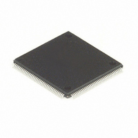
MC68HC16Z1CPV25 Freescale Semiconductor, MC68HC16Z1CPV25 Datasheet - Page 140

MC68HC16Z1CPV25
Manufacturer Part Number
MC68HC16Z1CPV25
Description
IC MPU 1K RAM 25MHZ 144-LQFP
Manufacturer
Freescale Semiconductor
Series
HC16r
Datasheet
1.MC68HC16Z1VEH16.pdf
(500 pages)
Specifications of MC68HC16Z1CPV25
Core Processor
CPU16
Core Size
16-Bit
Speed
25MHz
Connectivity
EBI/EMI, SCI, SPI
Peripherals
POR, PWM, WDT
Number Of I /o
16
Program Memory Type
ROMless
Ram Size
1K x 8
Voltage - Supply (vcc/vdd)
2.7 V ~ 5.5 V
Data Converters
A/D 8x10b
Oscillator Type
Internal
Operating Temperature
-40°C ~ 85°C
Package / Case
144-LQFP
Lead Free Status / RoHS Status
Contains lead / RoHS non-compliant
Eeprom Size
-
Program Memory Size
-
Other names
Q1141110
Available stocks
Company
Part Number
Manufacturer
Quantity
Price
Company:
Part Number:
MC68HC16Z1CPV25
Manufacturer:
MOT
Quantity:
5 510
Company:
Part Number:
MC68HC16Z1CPV25
Manufacturer:
SIEMENS
Quantity:
5 510
Company:
Part Number:
MC68HC16Z1CPV25
Manufacturer:
FREESCAL
Quantity:
624
Company:
Part Number:
MC68HC16Z1CPV25
Manufacturer:
Freescale Semiconductor
Quantity:
10 000
- Current page: 140 of 500
- Download datasheet (6Mb)
5-34
If the CPU is executing an instruction that reads a long-word operand from a 16-bit
port, the MCU latches the 16 bits of valid data and then runs another bus cycle to ob-
tain the other 16 bits. The operation for an 8-bit port is similar, but requires four read
cycles. The addressed device uses the DSACK signals to indicate the port width. For
instance, a 16-bit external device always returns DSACK for a 16-bit port (regardless
of whether the bus cycle is a byte or word operation).
Dynamic bus sizing requires that the portion of the data bus used for a transfer to or
from a particular port size be fixed. A 16-bit port must reside on data bus bits [15:0],
and an 8-bit port must reside on data bus bits [15:8]. This minimizes the number of bus
cycles needed to transfer data and ensures that the MCU transfers valid data.
The MCU always attempts to transfer the maximum amount of data on all bus cycles.
For a word operation, it is assumed that the port is 16 bits wide when the bus cycle
begins.
Operand bytes are designated as shown in
of access. For instance, OP0 is the most significant byte of a long-word operand, and
is accessed first, while OP3, the least significant byte, is accessed last. The two bytes
of a word-length operand are OP0 (most significant) and OP1. The single byte of a
byte-length operand is OP0.
OPERAND
LONG WORD
THREE BYTE
WORD
BYTE
DSACK1
31
1
1
0
0
OP0
Freescale Semiconductor, Inc.
Table 5-15 Effect of DSACK Signals
For More Information On This Product,
Figure 5-11 Operand Byte Order
DSACK0
24
SYSTEM INTEGRATION MODULE
1
0
1
0
23
Go to: www.freescale.com
OP1
OP0
Complete cycle — Data bus port size is sixteen bits
Complete cycle — Data bus port size is eight bits
BYTE ORDER
Insert wait states in current bus cycle
16 15
Figure
5-11. OP[0:3] represent the order
OP2
OP1
OP0
Reserved
Result
8 7
M68HC16 Z SERIES
OP3
OP2
OP1
OP0
USER’S MANUAL
OPERAND BYTE ORDER
0
Related parts for MC68HC16Z1CPV25
Image
Part Number
Description
Manufacturer
Datasheet
Request
R
Part Number:
Description:
Manufacturer:
Freescale Semiconductor, Inc
Datasheet:
Part Number:
Description:
Manufacturer:
Freescale Semiconductor, Inc
Datasheet:
Part Number:
Description:
Manufacturer:
Freescale Semiconductor, Inc
Datasheet:
Part Number:
Description:
Manufacturer:
Freescale Semiconductor, Inc
Datasheet:
Part Number:
Description:
Manufacturer:
Freescale Semiconductor, Inc
Datasheet:
Part Number:
Description:
Manufacturer:
Freescale Semiconductor, Inc
Datasheet:
Part Number:
Description:
Manufacturer:
Freescale Semiconductor, Inc
Datasheet:
Part Number:
Description:
Manufacturer:
Freescale Semiconductor, Inc
Datasheet:
Part Number:
Description:
Manufacturer:
Freescale Semiconductor, Inc
Datasheet:
Part Number:
Description:
Manufacturer:
Freescale Semiconductor, Inc
Datasheet:
Part Number:
Description:
Manufacturer:
Freescale Semiconductor, Inc
Datasheet:
Part Number:
Description:
Manufacturer:
Freescale Semiconductor, Inc
Datasheet:
Part Number:
Description:
Manufacturer:
Freescale Semiconductor, Inc
Datasheet:
Part Number:
Description:
Manufacturer:
Freescale Semiconductor, Inc
Datasheet:
Part Number:
Description:
Manufacturer:
Freescale Semiconductor, Inc
Datasheet:


