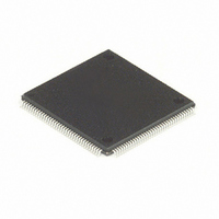
MC68HC16Z1CPV25 Freescale Semiconductor, MC68HC16Z1CPV25 Datasheet - Page 276

MC68HC16Z1CPV25
Manufacturer Part Number
MC68HC16Z1CPV25
Description
IC MPU 1K RAM 25MHZ 144-LQFP
Manufacturer
Freescale Semiconductor
Series
HC16r
Datasheet
1.MC68HC16Z1VEH16.pdf
(500 pages)
Specifications of MC68HC16Z1CPV25
Core Processor
CPU16
Core Size
16-Bit
Speed
25MHz
Connectivity
EBI/EMI, SCI, SPI
Peripherals
POR, PWM, WDT
Number Of I /o
16
Program Memory Type
ROMless
Ram Size
1K x 8
Voltage - Supply (vcc/vdd)
2.7 V ~ 5.5 V
Data Converters
A/D 8x10b
Oscillator Type
Internal
Operating Temperature
-40°C ~ 85°C
Package / Case
144-LQFP
Lead Free Status / RoHS Status
Contains lead / RoHS non-compliant
Eeprom Size
-
Program Memory Size
-
Other names
Q1141110
Available stocks
Company
Part Number
Manufacturer
Quantity
Price
Company:
Part Number:
MC68HC16Z1CPV25
Manufacturer:
MOT
Quantity:
5 510
Company:
Part Number:
MC68HC16Z1CPV25
Manufacturer:
SIEMENS
Quantity:
5 510
Company:
Part Number:
MC68HC16Z1CPV25
Manufacturer:
FREESCAL
Quantity:
624
Company:
Part Number:
MC68HC16Z1CPV25
Manufacturer:
Freescale Semiconductor
Quantity:
10 000
- Current page: 276 of 500
- Download datasheet (6Mb)
Freescale Semiconductor, Inc.
Edge-detection logic consists of control bits that enable edge detection and select a
transition to detect. The EDGExA/B bits in timer control register 2 (TCTL2) determine
whether the input capture functions detect rising edges only, falling edges only, or both
rising and falling edges. Clearing both bits disables the input capture function. Input
capture functions operate independently of each other and can capture the same
TCNT value if individual input edges are detected within the same timer count cycle.
Input capture interrupt logic includes a status flag, which indicates that an edge has
been detected, and an interrupt enable bit. An input capture event sets the ICxF bit in
the timer interrupt flag register 1 (TFLG1) and causes the GPT to make an interrupt
request if the corresponding ICxI bit is set in the timer interrupt mask register 1
(TMSK1). If the ICxI bit is cleared, software must poll the status flag to determine that
an event has occurred. Refer to
11.4 Polled and Interrupt-Driven Operation
for
more information.
Input capture events are generally asynchronous to the timer counter. Because of this,
input capture signals are conditioned by a synchronizer and digital filter. Events are
synchronized with the system clock and digital filter. Events are synchronized with the
system clock so that latching of TCNT content and counter incrementation occur on
opposite half-cycles of the system clock. Inputs have hysteresis. Capture of any tran-
sition longer than two system clocks is guaranteed; any transition shorter than one
system clock has no effect.
Figure 11-4
shows the relationship of system clock to synchronizer output. The value
latched into the capture register is the value of the counter several system clock cycles
after the transition that triggers the edge detection logic. There can be up to one clock
cycle of uncertainty in latching of the input transition. Maximum time is determined by
the system clock frequency.
The input capture register is a 16-bit register. A word access is required to ensure co-
herency. If coherency is not required, byte accesses can be used to read the register.
Input capture registers can be read at any time without affecting their values.
GENERAL-PURPOSE TIMER
M68HC16 Z SERIES
11-12
USER’S MANUAL
For More Information On This Product,
Go to: www.freescale.com
Related parts for MC68HC16Z1CPV25
Image
Part Number
Description
Manufacturer
Datasheet
Request
R
Part Number:
Description:
Manufacturer:
Freescale Semiconductor, Inc
Datasheet:
Part Number:
Description:
Manufacturer:
Freescale Semiconductor, Inc
Datasheet:
Part Number:
Description:
Manufacturer:
Freescale Semiconductor, Inc
Datasheet:
Part Number:
Description:
Manufacturer:
Freescale Semiconductor, Inc
Datasheet:
Part Number:
Description:
Manufacturer:
Freescale Semiconductor, Inc
Datasheet:
Part Number:
Description:
Manufacturer:
Freescale Semiconductor, Inc
Datasheet:
Part Number:
Description:
Manufacturer:
Freescale Semiconductor, Inc
Datasheet:
Part Number:
Description:
Manufacturer:
Freescale Semiconductor, Inc
Datasheet:
Part Number:
Description:
Manufacturer:
Freescale Semiconductor, Inc
Datasheet:
Part Number:
Description:
Manufacturer:
Freescale Semiconductor, Inc
Datasheet:
Part Number:
Description:
Manufacturer:
Freescale Semiconductor, Inc
Datasheet:
Part Number:
Description:
Manufacturer:
Freescale Semiconductor, Inc
Datasheet:
Part Number:
Description:
Manufacturer:
Freescale Semiconductor, Inc
Datasheet:
Part Number:
Description:
Manufacturer:
Freescale Semiconductor, Inc
Datasheet:
Part Number:
Description:
Manufacturer:
Freescale Semiconductor, Inc
Datasheet:


