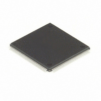
MC68HC16Z1CPV25 Freescale Semiconductor, MC68HC16Z1CPV25 Datasheet - Page 432

MC68HC16Z1CPV25
Manufacturer Part Number
MC68HC16Z1CPV25
Description
IC MPU 1K RAM 25MHZ 144-LQFP
Manufacturer
Freescale Semiconductor
Series
HC16r
Datasheet
1.MC68HC16Z1VEH16.pdf
(500 pages)
Specifications of MC68HC16Z1CPV25
Core Processor
CPU16
Core Size
16-Bit
Speed
25MHz
Connectivity
EBI/EMI, SCI, SPI
Peripherals
POR, PWM, WDT
Number Of I /o
16
Program Memory Type
ROMless
Ram Size
1K x 8
Voltage - Supply (vcc/vdd)
2.7 V ~ 5.5 V
Data Converters
A/D 8x10b
Oscillator Type
Internal
Operating Temperature
-40°C ~ 85°C
Package / Case
144-LQFP
Lead Free Status / RoHS Status
Contains lead / RoHS non-compliant
Eeprom Size
-
Program Memory Size
-
Other names
Q1141110
Available stocks
Company
Part Number
Manufacturer
Quantity
Price
Company:
Part Number:
MC68HC16Z1CPV25
Manufacturer:
MOT
Quantity:
5 510
Company:
Part Number:
MC68HC16Z1CPV25
Manufacturer:
SIEMENS
Quantity:
5 510
Company:
Part Number:
MC68HC16Z1CPV25
Manufacturer:
FREESCAL
Quantity:
624
Company:
Part Number:
MC68HC16Z1CPV25
Manufacturer:
Freescale Semiconductor
Quantity:
10 000
- Current page: 432 of 500
- Download datasheet (6Mb)
D.7.7 MCCI Data Direction Register
MDDR — MCCI Data Direction Register
D-58
RESET:
15
MDDR determines whether pins configured for general-purpose I/O are inputs or out-
puts. MDDR affects both SPI function and I/O function. During reset, all MCCI pins are
configured as inputs.
NOTES:
MCCI Pin
RXDB
TXDB
TXDA
RXDA
MISO
MOSI
SCK
1. SCK is automatically assigned to the SPI whenever the SPI is enabled (when the SPE
2. PMC4 and PMC6 function as general-purpose I/O pins when the corresponding RE bit
3. PMC5 and PMC7 function as general-purpose I/O pins when the corresponding TE bit
SS
bit in the SPCR1 is set).
in the SCI control register (SCCR0A or SCCR0B) is cleared.
in the SCI control register (SCCR0A or SCCR0B) is cleared.
1
3
3
2
Table D-40 Effect of MDDR on MCCI Pin Function
NOT USED
Master
Master
Master
Master
Mode
Slave
Slave
Slave
Slave
Freescale Semiconductor, Inc.
—
—
—
—
Table D-40
For More Information On This Product,
MDDR Bit
Go to: www.freescale.com
DDR0
DDR1
DDR2
DDR3
DDR4
DDR5
DDR6
DDR7
REGISTER SUMMARY
shows the effect of MDDR on MCCI pin function.
8
Bit State
DDR7
7
0
—
—
0
1
0
1
0
1
0
1
0
1
0
1
0
1
0
1
0
1
0
1
DDR6
6
0
Serial data output from SCIB
Serial data output from SCIA
Assertion causes mode fault
Serial data output from SPI
Serial data output from SPI
Disables slave-select input
Serial data input to SCIB
Serial data input to SCIA
DDR5
Serial data input to SPI
Serial data input to SPI
Clock output from SPI
SPI slave-select input
5
0
Disables data output
Disables data output
General-purpose I/O
General-purpose I/O
General-purpose I/O
General-purpose I/O
General-purpose I/O
Disables data input
Disables data input
Clock input to SPI
Pin Function
DDR4
4
0
DDR3
3
0
M68HC16 Z SERIES
USER’S MANUAL
DDR2
2
0
$YFFC0A
DDR1
1
0
DDR0
0
0
Related parts for MC68HC16Z1CPV25
Image
Part Number
Description
Manufacturer
Datasheet
Request
R
Part Number:
Description:
Manufacturer:
Freescale Semiconductor, Inc
Datasheet:
Part Number:
Description:
Manufacturer:
Freescale Semiconductor, Inc
Datasheet:
Part Number:
Description:
Manufacturer:
Freescale Semiconductor, Inc
Datasheet:
Part Number:
Description:
Manufacturer:
Freescale Semiconductor, Inc
Datasheet:
Part Number:
Description:
Manufacturer:
Freescale Semiconductor, Inc
Datasheet:
Part Number:
Description:
Manufacturer:
Freescale Semiconductor, Inc
Datasheet:
Part Number:
Description:
Manufacturer:
Freescale Semiconductor, Inc
Datasheet:
Part Number:
Description:
Manufacturer:
Freescale Semiconductor, Inc
Datasheet:
Part Number:
Description:
Manufacturer:
Freescale Semiconductor, Inc
Datasheet:
Part Number:
Description:
Manufacturer:
Freescale Semiconductor, Inc
Datasheet:
Part Number:
Description:
Manufacturer:
Freescale Semiconductor, Inc
Datasheet:
Part Number:
Description:
Manufacturer:
Freescale Semiconductor, Inc
Datasheet:
Part Number:
Description:
Manufacturer:
Freescale Semiconductor, Inc
Datasheet:
Part Number:
Description:
Manufacturer:
Freescale Semiconductor, Inc
Datasheet:
Part Number:
Description:
Manufacturer:
Freescale Semiconductor, Inc
Datasheet:


