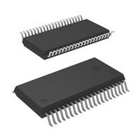
M30263F6AFP#U3 Renesas Electronics America, M30263F6AFP#U3 Datasheet - Page 106

M30263F6AFP#U3
Manufacturer Part Number
M30263F6AFP#U3
Description
MCU 3/5V 48K I TEMP PB-FREE 42-S
Manufacturer
Renesas Electronics America
Series
M16C™ M16C/Tiny/26r
Datasheet
1.M30260F3AGPU5A.pdf
(354 pages)
Specifications of M30263F6AFP#U3
Core Processor
M16C/60
Core Size
16-Bit
Speed
20MHz
Connectivity
I²C, IEBus, SIO, UART/USART
Peripherals
DMA, PWM, Voltage Detect, WDT
Number Of I /o
33
Program Memory Size
48KB (48K x 8)
Program Memory Type
FLASH
Ram Size
2K x 8
Voltage - Supply (vcc/vdd)
2.7 V ~ 5.5 V
Data Converters
A/D 10x10b
Oscillator Type
Internal
Operating Temperature
-40°C ~ 85°C
Package / Case
42-SSOP
Lead Free Status / RoHS Status
Lead free / RoHS Compliant
Eeprom Size
-
- Current page: 106 of 354
- Download datasheet (4Mb)
R
R
M
e
E
11.1 Transfer Cycles
. v
J
1
0
6
The transfer cycle consists of a memory or SFR read (source read) bus cycle and a write (destination write)
bus cycle. The number of read and write bus cycles is affected by the source and destination addresses of
transfer. Furthermore, the bus cycle itself is extended by a software wait.
11.1.1 Effect of Source and Destination Addresses
11.1.2 Effect of Software Wait
Figure 11.1.1 shows the example of the cycles for a source read. For convenience, the destination write
cycle is shown as one cycle and the source read cycles for the different conditions are shown. In reality, the
destination write cycle is subject to the same conditions as the source read cycle, with the transfer cycle
changing accordingly. When calculating transfer cycles, take into consideration each condition for the
source read and the destination write cycle, respectively. For example, when data is transferred in 16 bit
units and when both the source address and destination address are an odd address ((2) in Figure 11.1.1),
two source read bus cycles and two destination write bus cycles are required.
2
9
C
0 .
B
If the transfer unit is 16 bits and the source address of transfer begins with an odd address, the source
read cycle consists of one more bus cycle than when the source address of transfer begins with an even
address.
Similarly, if the transfer unit is 16 bits and the destination address of transfer begins with an odd address,
the destination write cycle consists of one more bus cycle than when the destination address of transfer
begins with an even address.
For memory or SFR accesses in which one or more software wait states are inserted, the number of bus
cycles required for that access increases by an amount equal to software wait states.
2 /
0
0
2
6
0
F
A
2
e
0 -
b
G
1 .
2
o r
0
, 5
0
u
2
p
0
(
0
M
7
1
6
page 87
C
2 /
6
, A
M
f o
1
6
3
C
2
9
2 /
6
, B
M
1
6
C
2 /
6
) T
11. DMAC
Related parts for M30263F6AFP#U3
Image
Part Number
Description
Manufacturer
Datasheet
Request
R

Part Number:
Description:
KIT STARTER FOR M16C/29
Manufacturer:
Renesas Electronics America
Datasheet:

Part Number:
Description:
KIT STARTER FOR R8C/2D
Manufacturer:
Renesas Electronics America
Datasheet:

Part Number:
Description:
R0K33062P STARTER KIT
Manufacturer:
Renesas Electronics America
Datasheet:

Part Number:
Description:
KIT STARTER FOR R8C/23 E8A
Manufacturer:
Renesas Electronics America
Datasheet:

Part Number:
Description:
KIT STARTER FOR R8C/25
Manufacturer:
Renesas Electronics America
Datasheet:

Part Number:
Description:
KIT STARTER H8S2456 SHARPE DSPLY
Manufacturer:
Renesas Electronics America
Datasheet:

Part Number:
Description:
KIT STARTER FOR R8C38C
Manufacturer:
Renesas Electronics America
Datasheet:

Part Number:
Description:
KIT STARTER FOR R8C35C
Manufacturer:
Renesas Electronics America
Datasheet:

Part Number:
Description:
KIT STARTER FOR R8CL3AC+LCD APPS
Manufacturer:
Renesas Electronics America
Datasheet:

Part Number:
Description:
KIT STARTER FOR RX610
Manufacturer:
Renesas Electronics America
Datasheet:

Part Number:
Description:
KIT STARTER FOR R32C/118
Manufacturer:
Renesas Electronics America
Datasheet:

Part Number:
Description:
KIT DEV RSK-R8C/26-29
Manufacturer:
Renesas Electronics America
Datasheet:

Part Number:
Description:
KIT STARTER FOR SH7124
Manufacturer:
Renesas Electronics America
Datasheet:

Part Number:
Description:
KIT STARTER FOR H8SX/1622
Manufacturer:
Renesas Electronics America
Datasheet:

Part Number:
Description:
KIT DEV FOR SH7203
Manufacturer:
Renesas Electronics America
Datasheet:


