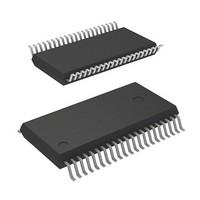
M30263F6AFP#U3 Renesas Electronics America, M30263F6AFP#U3 Datasheet - Page 175

M30263F6AFP#U3
Manufacturer Part Number
M30263F6AFP#U3
Description
MCU 3/5V 48K I TEMP PB-FREE 42-S
Manufacturer
Renesas Electronics America
Series
M16C™ M16C/Tiny/26r
Datasheet
1.M30260F3AGPU5A.pdf
(354 pages)
Specifications of M30263F6AFP#U3
Core Processor
M16C/60
Core Size
16-Bit
Speed
20MHz
Connectivity
I²C, IEBus, SIO, UART/USART
Peripherals
DMA, PWM, Voltage Detect, WDT
Number Of I /o
33
Program Memory Size
48KB (48K x 8)
Program Memory Type
FLASH
Ram Size
2K x 8
Voltage - Supply (vcc/vdd)
2.7 V ~ 5.5 V
Data Converters
A/D 10x10b
Oscillator Type
Internal
Operating Temperature
-40°C ~ 85°C
Package / Case
42-SSOP
Lead Free Status / RoHS Status
Lead free / RoHS Compliant
Eeprom Size
-
- Current page: 175 of 354
- Download datasheet (4Mb)
R
R
M
e
E
. v
1
J
Figure 13.1.2.4.1. Serial Data Logic Switching
Figure 13.1.2.5.1. T
6
0
2
9
C
0 .
B
2 /
0
0
13.1.2.4. Serial Data Logic Switching Function (UART2)
13.1.2.5. TxD and RxD I/O Polarity Inverse Function (UART2)
2
6
(1) When the U2LCH bit in the U2C1 register is set to "0" (no reverse)
(2) When the U2LCH bit in the U2C1 register is set "1" (reverse)
0
The data written to the U2TB register has its logic reversed before being transmitted. Similarly, the
received data has its logic reversed when read from the U2RB register. Figure 13.1.2.4.1 shows serial
data logic.
This function inverses the polarities of the T
input/output data (including the start, stop and parity bits) are inversed. Figure 13.1.2.5.1 shows the
T
A
NOTE:
F
Transfer clock
Transfer clock
2
(1) When the IOPOL bit in the U2MR register is set to "0" (no reverse)
(2) When the IOPOL bit in the U2MR register is set to "1" (reverse)
X
e
NOTE:
0 -
G
b
D pin output and R
1. This applies to the case where the CKPOL bit in the U2C0 register is set to "0"
Transfer clock
Transfer clock
(no reverse)
1 .
2
o r
(reverse)
(transmit data output at the falling edge of the transfer clock), the UFORM bit in the
U2C0 register is set to "0" (LSB first), the STPS bit in the U2MR register is set to "0"
(1 stop bit) and the PRYE bit in the U2MR register is set to "1" (parity enabled).
1. This applies to the case where the UFORM bit in the U2C0 register is set to
0
(no reverse)
(no reverse)
, 5
u
0
TxD
"0"(LSB first), the STPS bit in the U2MR register is set to "0" (1 stop bit) and the
PRYE bit in the U2MR register is set to "1"(parity enabled).
TxD
(reverse)
p
(reverse)
2
0
RxD
(
RxD
TxD
TxD
2
2
M
0
7
1
2
2
2
2
“H”
“H”
“H”
“L”
“H”
“L”
“L”
6
“L”
“H”
“L”
“H”
“L”
“H”
“L”
“H”
C
“L”
“H”
“H”
“L”
“L”
page 156
X
D and R
2 /
6
, A
ST
ST
X
M
ST
ST
ST
ST
D pin input polarity inverse.
f o
1
X
6
D0
D0
D I/O Polarity Inverse
3
C
D0
D0
D0
D0
2
2 /
9
D1
6
D1
, B
D1
D1
D1
D1
D2
M
D2
1
D2
D2
D2
D2
6
D3
C
D3
2 /
D3
D3
D3
D3
6
D4
D4
) T
X
D2 pin output and R
D4
D4
D4
D4
D5
D5
D5
D5
D5
D5
D6
D6
D6
D6
D6
D6
D7
D7
D7
D7
D7
D7
P
P
SP
P
P
P
P
SP
X
D2 pin input. The logic levels of all
SP
SP
SP
SP
ST: Start bit
P: Parity bit
SP: Stop bit
ST: Start bit
P: Parity bit
SP: Stop bit
13. Serial I/O
Related parts for M30263F6AFP#U3
Image
Part Number
Description
Manufacturer
Datasheet
Request
R

Part Number:
Description:
KIT STARTER FOR M16C/29
Manufacturer:
Renesas Electronics America
Datasheet:

Part Number:
Description:
KIT STARTER FOR R8C/2D
Manufacturer:
Renesas Electronics America
Datasheet:

Part Number:
Description:
R0K33062P STARTER KIT
Manufacturer:
Renesas Electronics America
Datasheet:

Part Number:
Description:
KIT STARTER FOR R8C/23 E8A
Manufacturer:
Renesas Electronics America
Datasheet:

Part Number:
Description:
KIT STARTER FOR R8C/25
Manufacturer:
Renesas Electronics America
Datasheet:

Part Number:
Description:
KIT STARTER H8S2456 SHARPE DSPLY
Manufacturer:
Renesas Electronics America
Datasheet:

Part Number:
Description:
KIT STARTER FOR R8C38C
Manufacturer:
Renesas Electronics America
Datasheet:

Part Number:
Description:
KIT STARTER FOR R8C35C
Manufacturer:
Renesas Electronics America
Datasheet:

Part Number:
Description:
KIT STARTER FOR R8CL3AC+LCD APPS
Manufacturer:
Renesas Electronics America
Datasheet:

Part Number:
Description:
KIT STARTER FOR RX610
Manufacturer:
Renesas Electronics America
Datasheet:

Part Number:
Description:
KIT STARTER FOR R32C/118
Manufacturer:
Renesas Electronics America
Datasheet:

Part Number:
Description:
KIT DEV RSK-R8C/26-29
Manufacturer:
Renesas Electronics America
Datasheet:

Part Number:
Description:
KIT STARTER FOR SH7124
Manufacturer:
Renesas Electronics America
Datasheet:

Part Number:
Description:
KIT STARTER FOR H8SX/1622
Manufacturer:
Renesas Electronics America
Datasheet:

Part Number:
Description:
KIT DEV FOR SH7203
Manufacturer:
Renesas Electronics America
Datasheet:


