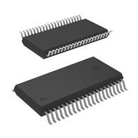
M30263F6AFP#U3 Renesas Electronics America, M30263F6AFP#U3 Datasheet - Page 65

M30263F6AFP#U3
Manufacturer Part Number
M30263F6AFP#U3
Description
MCU 3/5V 48K I TEMP PB-FREE 42-S
Manufacturer
Renesas Electronics America
Series
M16C™ M16C/Tiny/26r
Datasheet
1.M30260F3AGPU5A.pdf
(354 pages)
Specifications of M30263F6AFP#U3
Core Processor
M16C/60
Core Size
16-Bit
Speed
20MHz
Connectivity
I²C, IEBus, SIO, UART/USART
Peripherals
DMA, PWM, Voltage Detect, WDT
Number Of I /o
33
Program Memory Size
48KB (48K x 8)
Program Memory Type
FLASH
Ram Size
2K x 8
Voltage - Supply (vcc/vdd)
2.7 V ~ 5.5 V
Data Converters
A/D 10x10b
Oscillator Type
Internal
Operating Temperature
-40°C ~ 85°C
Package / Case
42-SSOP
Lead Free Status / RoHS Status
Lead free / RoHS Compliant
Eeprom Size
-
- Current page: 65 of 354
- Download datasheet (4Mb)
R
R
M
e
E
7.2 Sub Clock
. v
J
1
Figure 7.2.1. Examples of Sub Clock Connection Circuit
0
6
2
The sub clock is generated by the sub clock oscillation circuit. This clock is used as the clock source for the
CPU clock, as well as the timer A and timer B count sources.
The sub clock oscillator circuit is configured by connecting a crystal resonator between the X
pins. The sub clock oscillator circuit contains a feedback resistor, which is disconnected from the oscillator
circuit during stop mode in order to reduce the amount of power consumed in the chip. The sub clock
oscillator circuit may also be configured by feeding an externally generated clock to the X
7.2.1 shows the examples of sub clock connection circuit.
After reset, the sub clock is turned off. At this time, the feedback resistor is disconnected from the oscillator
circuit.
To use the sub clock for the CPU clock, set the CM07 bit in the CM0 register to “1 ” (sub clock) after the sub
clock becomes oscillating stably.
During stop mode, all clocks including the sub clock are turned off. Refer to 7.6 Power Control.
9
C
0 .
B
2 /
0
0
2
6
0
F
A
2
e
0 -
b
G
1 .
2
o r
(Built-in Feedback Resistor)
0
, 5
0
u
2
p
0
(
0
M
7
NOTE:
1
6
MCU
1. Place a damping resistor if required. Resistance values vary depending on the oscillator setting.
C
page 46
X
Use values recommended by each oscillator manufacturer.
Place a feedback resistor between X
placing the resistor externally.
2 /
COUT
X
V
6
CIN
SS
, A
M
f o
1
Oscillator
6
3
R
C
2
C
9
2 /
d
(1)
6
, B
M
1
C
C
6
COUT
CIN
C
2 /
6
CIN
) T
and X
(Built-in Feedback Resistor)
COUT
if the oscillator manufacturer recommends
MCU
X
C OUT
X
C IN
Open
V
V
CC
SS
External Clock
7. Clock Generation Circuit
CIN
CIN
and X
pin. Figure
COUT
Related parts for M30263F6AFP#U3
Image
Part Number
Description
Manufacturer
Datasheet
Request
R

Part Number:
Description:
KIT STARTER FOR M16C/29
Manufacturer:
Renesas Electronics America
Datasheet:

Part Number:
Description:
KIT STARTER FOR R8C/2D
Manufacturer:
Renesas Electronics America
Datasheet:

Part Number:
Description:
R0K33062P STARTER KIT
Manufacturer:
Renesas Electronics America
Datasheet:

Part Number:
Description:
KIT STARTER FOR R8C/23 E8A
Manufacturer:
Renesas Electronics America
Datasheet:

Part Number:
Description:
KIT STARTER FOR R8C/25
Manufacturer:
Renesas Electronics America
Datasheet:

Part Number:
Description:
KIT STARTER H8S2456 SHARPE DSPLY
Manufacturer:
Renesas Electronics America
Datasheet:

Part Number:
Description:
KIT STARTER FOR R8C38C
Manufacturer:
Renesas Electronics America
Datasheet:

Part Number:
Description:
KIT STARTER FOR R8C35C
Manufacturer:
Renesas Electronics America
Datasheet:

Part Number:
Description:
KIT STARTER FOR R8CL3AC+LCD APPS
Manufacturer:
Renesas Electronics America
Datasheet:

Part Number:
Description:
KIT STARTER FOR RX610
Manufacturer:
Renesas Electronics America
Datasheet:

Part Number:
Description:
KIT STARTER FOR R32C/118
Manufacturer:
Renesas Electronics America
Datasheet:

Part Number:
Description:
KIT DEV RSK-R8C/26-29
Manufacturer:
Renesas Electronics America
Datasheet:

Part Number:
Description:
KIT STARTER FOR SH7124
Manufacturer:
Renesas Electronics America
Datasheet:

Part Number:
Description:
KIT STARTER FOR H8SX/1622
Manufacturer:
Renesas Electronics America
Datasheet:

Part Number:
Description:
KIT DEV FOR SH7203
Manufacturer:
Renesas Electronics America
Datasheet:


