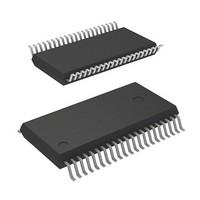
M30263F6AFP#U3 Renesas Electronics America, M30263F6AFP#U3 Datasheet - Page 160

M30263F6AFP#U3
Manufacturer Part Number
M30263F6AFP#U3
Description
MCU 3/5V 48K I TEMP PB-FREE 42-S
Manufacturer
Renesas Electronics America
Series
M16C™ M16C/Tiny/26r
Datasheet
1.M30260F3AGPU5A.pdf
(354 pages)
Specifications of M30263F6AFP#U3
Core Processor
M16C/60
Core Size
16-Bit
Speed
20MHz
Connectivity
I²C, IEBus, SIO, UART/USART
Peripherals
DMA, PWM, Voltage Detect, WDT
Number Of I /o
33
Program Memory Size
48KB (48K x 8)
Program Memory Type
FLASH
Ram Size
2K x 8
Voltage - Supply (vcc/vdd)
2.7 V ~ 5.5 V
Data Converters
A/D 10x10b
Oscillator Type
Internal
Operating Temperature
-40°C ~ 85°C
Package / Case
42-SSOP
Lead Free Status / RoHS Status
Lead free / RoHS Compliant
Eeprom Size
-
- Current page: 160 of 354
- Download datasheet (4Mb)
R
R
M
e
E
. v
1
J
Figure 13.1.9. U2SMR3 register and U2SMR4 register
0
6
2
9
C
0 .
B
2 /
0
0
2
6
0
A
F
2
UART2 special mode register 3
b7 b6 b5 b4 b3 b2 b1 b0
e
NOTES:
0 -
G
b
UART2 Special Mode Register 4
b7 b6 b5 b4 b3 b2 b1 b0
1 .
2
o r
NOTE:
1. The DL2 to DL0 bits are used to generate a delay in SDA2 output by digital means during I
2. The amount of delay varies with the load on SCL2 and SDA2 pins. Also, when using an external clock, the amount of
0
, 5
u
0
I
delay increases by about 100 ns.
1. Set to “0” when each condition is generated.
2
p
C bus mode, set these bits to “000
2
0
(
0
M
7
1
6
C
page 141
2 /
6
, A
M
symbol
CKPH
NODC
(b0)
(b2)
(b4)
DL0
DL1
DL2
1
f o
Bit
6
Bit Symbol
RSTAREQ
STSPSEL
3
C
STPREQ
STAREQ
2
SCLHI
SWC9
ACKD
ACKC
2 /
9
Nothing is assigned.
When write, set “0”. When read, its content is indeterminate.
Nothing is assigned.
When write, set “0”. When read, its content is indeterminate.
Nothing is assigned.
When write, set “0”. When read, its content is indeterminate.
U2SMR3
Clock phase set bit
Clock output select bit
SDA digital delay
setup bit
6
Symbol
U2SMR4
Symbol
, B
2
” (no delay).
M
Bit name
1
Restart condition
generate bit
Stop condition
SCL
ACK data bit
ACK data output
SCL
SCL
Start condition
generate bit
(1, 2)
6
C
2
2
2
2 /
, SDA
Bit Name
output stop
wait bit 3
6
) T
Address
0374
2
(1)
output
(1)
16
b7 b6 b5
0 : Without clock delay
1 : With clock delay
0 : CLKi is CMOS output
1 : CLKi is N-channel open drain output
0 0 0 : Without delay
0 0 1 : 1 to 2 cycle(s) of UiBRG count source
0 1 0 : 2 to 3 cycles of UiBRG count source
0 1 1 : 3 to 4 cycles of UiBRG count source
1 0 0 : 4 to 5 cycles of UiBRG count source
1 0 1 : 5 to 6 cycles of UiBRG count source
1 1 0 : 6 to 7 cycles of UiBRG count source
1 1 1 : 7 to 8 cycles of UiBRG count source
Address
0375
0: Clear
1: Start
0: Clear
1: Start
0: Clear
1: Start
0: Start and stop conditions not output
1: Start and stop conditions output
0: ACK
1: NACK
0: Serial I/O data output
1: ACK data output
0: Disabled
1: Enabled
0: SCL
1: SCL
16
After Reset
00
2
2
16
“L” hold disabled
“L” hold enabled
Function
000X0X0X
After reset
Function
2
C bus mode. In other than
2
RW
RW
RW
RW
RW
RW
RW
RW
RW
RW
RW
RW
RW
RW
RW
13. Serial I/O
Related parts for M30263F6AFP#U3
Image
Part Number
Description
Manufacturer
Datasheet
Request
R

Part Number:
Description:
KIT STARTER FOR M16C/29
Manufacturer:
Renesas Electronics America
Datasheet:

Part Number:
Description:
KIT STARTER FOR R8C/2D
Manufacturer:
Renesas Electronics America
Datasheet:

Part Number:
Description:
R0K33062P STARTER KIT
Manufacturer:
Renesas Electronics America
Datasheet:

Part Number:
Description:
KIT STARTER FOR R8C/23 E8A
Manufacturer:
Renesas Electronics America
Datasheet:

Part Number:
Description:
KIT STARTER FOR R8C/25
Manufacturer:
Renesas Electronics America
Datasheet:

Part Number:
Description:
KIT STARTER H8S2456 SHARPE DSPLY
Manufacturer:
Renesas Electronics America
Datasheet:

Part Number:
Description:
KIT STARTER FOR R8C38C
Manufacturer:
Renesas Electronics America
Datasheet:

Part Number:
Description:
KIT STARTER FOR R8C35C
Manufacturer:
Renesas Electronics America
Datasheet:

Part Number:
Description:
KIT STARTER FOR R8CL3AC+LCD APPS
Manufacturer:
Renesas Electronics America
Datasheet:

Part Number:
Description:
KIT STARTER FOR RX610
Manufacturer:
Renesas Electronics America
Datasheet:

Part Number:
Description:
KIT STARTER FOR R32C/118
Manufacturer:
Renesas Electronics America
Datasheet:

Part Number:
Description:
KIT DEV RSK-R8C/26-29
Manufacturer:
Renesas Electronics America
Datasheet:

Part Number:
Description:
KIT STARTER FOR SH7124
Manufacturer:
Renesas Electronics America
Datasheet:

Part Number:
Description:
KIT STARTER FOR H8SX/1622
Manufacturer:
Renesas Electronics America
Datasheet:

Part Number:
Description:
KIT DEV FOR SH7203
Manufacturer:
Renesas Electronics America
Datasheet:


