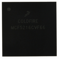
MCF5216CVF66 Freescale Semiconductor, MCF5216CVF66 Datasheet - Page 183

MCF5216CVF66
Manufacturer Part Number
MCF5216CVF66
Description
IC MPU 32BIT COLDF 256-MAPBGA
Manufacturer
Freescale Semiconductor
Series
MCF521xr
Datasheet
1.MCF5216CVM66J.pdf
(766 pages)
Specifications of MCF5216CVF66
Core Processor
Coldfire V2
Core Size
32-Bit
Speed
66MHz
Connectivity
CAN, EBI/EMI, I²C, SPI, UART/USART
Peripherals
DMA, LVD, POR, PWM, WDT
Number Of I /o
142
Program Memory Size
512KB (512K x 8)
Program Memory Type
FLASH
Ram Size
64K x 8
Voltage - Supply (vcc/vdd)
2.7 V ~ 3.6 V
Data Converters
A/D 8x12b
Oscillator Type
Internal
Operating Temperature
-40°C ~ 85°C
Package / Case
256-MAPBGA
Controller Family/series
ColdFire
Ram Memory Size
64KB
Embedded Interface Type
CAN, I2C, SPI, UART
No. Of Pwm Channels
8
Operating Temperature Range
-40°C To +85°C
No. Of Pins
256
Rohs Compliant
No
Package
256MA-BGA
Device Core
ColdFire
Family Name
MCF521x
Maximum Speed
66 MHz
Operating Supply Voltage
3.3 V
Data Bus Width
32 Bit
Number Of Programmable I/os
142
Interface Type
QSPI/UART/I2C/CAN
On-chip Adc
8-chx10-bit
Number Of Timers
8
Lead Free Status / RoHS Status
Contains lead / RoHS non-compliant
Eeprom Size
-
Available stocks
Company
Part Number
Manufacturer
Quantity
Price
Company:
Part Number:
MCF5216CVF66
Manufacturer:
FSC
Quantity:
1 670
Company:
Part Number:
MCF5216CVF66
Manufacturer:
Freescale Semiconductor
Quantity:
10 000
Part Number:
MCF5216CVF66
Manufacturer:
FREESCALE
Quantity:
20 000
Company:
Part Number:
MCF5216CVF66J
Manufacturer:
Freescale Semiconductor
Quantity:
10 000
- Current page: 183 of 766
- Download datasheet (9Mb)
The feedback clock comes from one of the following:
When the frequency of the feedback clock equals the frequency of the reference clock, the PLL is
frequency-locked. If the falling edge of the feedback clock lags the falling edge of the reference clock, the
PFD pulses the UP signal. If the falling edge of the feedback clock leads the falling edge of the reference
clock, the PFD pulses the DOWN signal. The width of these pulses relative to the reference clock depends
on how much the two clocks lead or lag each other. Once phase lock is achieved, the PFD continues to
pulse the UP and DOWN signals for very short durations during each reference clock cycle. These short
pulses continually update the PLL and prevent the frequency drift phenomenon known as dead-banding.
9.7.4.2
In 1:1 PLL mode, the charge pump uses a fixed current. In normal mode the current magnitude of the
charge pump varies with the MFD as shown in
The UP and DOWN signals from the PFD control whether the charge pump applies or removes charge,
respectively, from the loop filter. The filter is integrated on the chip.
9.7.4.3
The voltage across the loop filter controls the frequency of the VCO output. The frequency-to-voltage
relationship (VCO gain) is positive, and the output frequency is four times the target system frequency.
9.7.4.4
When the PLL is not in 1:1 PLL mode, the MFD divides the output of the VCO and feeds it back to the
PFD. The PFD controls the VCO frequency via the charge pump and loop filter such that the reference and
feedback clocks have the same frequency and phase. Thus, the frequency of the input to the MFD, which
is also the output of the VCO, is the reference frequency multiplied by the same amount that the MFD
divides by. For example, if the MFD divides the VCO frequency by six, the PLL is frequency locked when
the VCO frequency is six times the reference frequency. The presence of the MFD in the loop allows the
PLL to perform frequency multiplication, or synthesis.
In 1:1 PLL mode, the MFD is bypassed, and the effective multiplication factor is one.
9.7.4.5
The lock detect logic monitors the reference frequency and the PLL feedback frequency to determine when
frequency lock is achieved. Phase lock is inferred by the frequency relationship, but is not guaranteed. The
LOCK flag in the SYNSR reflects the PLL lock status. A sticky lock flag, LOCKS, is also provided.
Freescale Semiconductor
•
•
•
CLKOUT in 1:1 PLL mode
VCO output divided by two if CLKOUT is disabled in 1:1 PLL mode
VCO output divided by the MFD in normal PLL mode
Charge Pump/Loop Filter
Voltage Control Output (VCO)
Multiplication Factor Divider (MFD)
PLL Lock Detection
Table 9-8. Charge Pump Current and MFD in Normal Mode Operation
MCF5282 and MCF5216 ColdFire Microcontroller User’s Manual, Rev. 3
Charge Pump Current
1X
2X
4X
Table
9-8.
0 ≤ MFD < 2
2 ≤ MFD < 6
6 ≤ MFD
MFD
Clock Module
9-13
Related parts for MCF5216CVF66
Image
Part Number
Description
Manufacturer
Datasheet
Request
R
Part Number:
Description:
Manufacturer:
Freescale Semiconductor, Inc
Datasheet:
Part Number:
Description:
Manufacturer:
Freescale Semiconductor, Inc
Datasheet:
Part Number:
Description:
Manufacturer:
Freescale Semiconductor, Inc
Datasheet:
Part Number:
Description:
Manufacturer:
Freescale Semiconductor, Inc
Datasheet:
Part Number:
Description:
Manufacturer:
Freescale Semiconductor, Inc
Datasheet:
Part Number:
Description:
Manufacturer:
Freescale Semiconductor, Inc
Datasheet:
Part Number:
Description:
Manufacturer:
Freescale Semiconductor, Inc
Datasheet:
Part Number:
Description:
Manufacturer:
Freescale Semiconductor, Inc
Datasheet:
Part Number:
Description:
Manufacturer:
Freescale Semiconductor, Inc
Datasheet:
Part Number:
Description:
Manufacturer:
Freescale Semiconductor, Inc
Datasheet:
Part Number:
Description:
Manufacturer:
Freescale Semiconductor, Inc
Datasheet:
Part Number:
Description:
Manufacturer:
Freescale Semiconductor, Inc
Datasheet:
Part Number:
Description:
Manufacturer:
Freescale Semiconductor, Inc
Datasheet:
Part Number:
Description:
Manufacturer:
Freescale Semiconductor, Inc
Datasheet:
Part Number:
Description:
Manufacturer:
Freescale Semiconductor, Inc
Datasheet:


