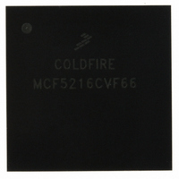
MCF5216CVF66 Freescale Semiconductor, MCF5216CVF66 Datasheet - Page 389

MCF5216CVF66
Manufacturer Part Number
MCF5216CVF66
Description
IC MPU 32BIT COLDF 256-MAPBGA
Manufacturer
Freescale Semiconductor
Series
MCF521xr
Datasheet
1.MCF5216CVM66J.pdf
(766 pages)
Specifications of MCF5216CVF66
Core Processor
Coldfire V2
Core Size
32-Bit
Speed
66MHz
Connectivity
CAN, EBI/EMI, I²C, SPI, UART/USART
Peripherals
DMA, LVD, POR, PWM, WDT
Number Of I /o
142
Program Memory Size
512KB (512K x 8)
Program Memory Type
FLASH
Ram Size
64K x 8
Voltage - Supply (vcc/vdd)
2.7 V ~ 3.6 V
Data Converters
A/D 8x12b
Oscillator Type
Internal
Operating Temperature
-40°C ~ 85°C
Package / Case
256-MAPBGA
Controller Family/series
ColdFire
Ram Memory Size
64KB
Embedded Interface Type
CAN, I2C, SPI, UART
No. Of Pwm Channels
8
Operating Temperature Range
-40°C To +85°C
No. Of Pins
256
Rohs Compliant
No
Package
256MA-BGA
Device Core
ColdFire
Family Name
MCF521x
Maximum Speed
66 MHz
Operating Supply Voltage
3.3 V
Data Bus Width
32 Bit
Number Of Programmable I/os
142
Interface Type
QSPI/UART/I2C/CAN
On-chip Adc
8-chx10-bit
Number Of Timers
8
Lead Free Status / RoHS Status
Contains lead / RoHS non-compliant
Eeprom Size
-
Available stocks
Company
Part Number
Manufacturer
Quantity
Price
Company:
Part Number:
MCF5216CVF66
Manufacturer:
FSC
Quantity:
1 670
Company:
Part Number:
MCF5216CVF66
Manufacturer:
Freescale Semiconductor
Quantity:
10 000
Part Number:
MCF5216CVF66
Manufacturer:
FREESCALE
Quantity:
20 000
Company:
Part Number:
MCF5216CVF66J
Manufacturer:
Freescale Semiconductor
Quantity:
10 000
- Current page: 389 of 766
- Download datasheet (9Mb)
1
2
3
4
5
6
20.7
Reset initializes the GPT registers to a known startup state as described in
and
20.8
Table 20-24
20.8.1
A channel flag is set when an input capture or output compare event occurs. Clear a channel flag by writing
a 1 to it.
Freescale Semiconductor
When DDR set the pin as input (0), reading the data register will return the state of the pin. When DDR set the pin as output (1),
reading the data register will return the content of the data latch. Pin conditions such as rising or falling edges can trigger an input
capture on a pin configured as an input.
OMn/OLn bit pairs select the output action to be taken as a result of a successful output compare. When either OMn or OLn is
set and the IOSn bit is set, the pin is an output regardless of the state of the corresponding DDR bit.
Setting an OC3M bit configures the corresponding PORTTn pin to be output. OC3Mn makes the PORTTn pin an output regardless
of the data direction bit when the pin is configured for output compare (IOSn = 1). The OC3Mn bits do not change the state of the
PORTTnDDR bits.
X = Don’t care
An output compare overrides the data direction bit of the output compare pin but does not change the state of the data direction
bit. Enabling output compare disables data register drive of the pin.
A successful output compare on channel 3 causes an output value determined by OC3Dn value to temporarily override the output
compare pin state of any other output compare channel.The next OC action for the specific channel will still be output to the pin.
A channel 3 output compare can cause bits in the output compare 3 data register to transfer to the GPT port data register,
depending on the output compare 3 mask register.
1
1
Registers.”
0
1
Reset
Interrupts
GPT Channel Interrupts (CnF)
lists the interrupt requests generated by the timer.
1
1
Channel 3 IC/OC
Channel 2 IC/OC
Channel 1 IC/OC
Channel 0 IC/OC
PA overflow
PA input
Timer overflow
X
X
Table 20-23. GPT Settings and Pin Functions (continued)
MCF5282 and MCF5216 ColdFire Microcontroller User’s Manual, Rev. 3
Interrupt Request
X
X
Table 20-24. GPT Interrupt Requests
1
1
Out
Out
PAOVF
Flag
PAIF
C3F
C2F
C1F
C0F
TOF
OC3Dn
OC3Dn
action/
action/
OC
OC
Output compare
compare/
OC3Dn
General Purpose Timer Modules (GPTA and GPTB)
Output
(ch 3)
(ch 3)
Enable Bit
PAOVI
TOI
C3I
C2I
C1I
C0I
PAI
Pin readable only if DDR = 0
Pin driven by channel OC action and
OC3Dn via channel 3 OC
Section 20.5, “Memory Map
(6)
6
20-21
Related parts for MCF5216CVF66
Image
Part Number
Description
Manufacturer
Datasheet
Request
R
Part Number:
Description:
Manufacturer:
Freescale Semiconductor, Inc
Datasheet:
Part Number:
Description:
Manufacturer:
Freescale Semiconductor, Inc
Datasheet:
Part Number:
Description:
Manufacturer:
Freescale Semiconductor, Inc
Datasheet:
Part Number:
Description:
Manufacturer:
Freescale Semiconductor, Inc
Datasheet:
Part Number:
Description:
Manufacturer:
Freescale Semiconductor, Inc
Datasheet:
Part Number:
Description:
Manufacturer:
Freescale Semiconductor, Inc
Datasheet:
Part Number:
Description:
Manufacturer:
Freescale Semiconductor, Inc
Datasheet:
Part Number:
Description:
Manufacturer:
Freescale Semiconductor, Inc
Datasheet:
Part Number:
Description:
Manufacturer:
Freescale Semiconductor, Inc
Datasheet:
Part Number:
Description:
Manufacturer:
Freescale Semiconductor, Inc
Datasheet:
Part Number:
Description:
Manufacturer:
Freescale Semiconductor, Inc
Datasheet:
Part Number:
Description:
Manufacturer:
Freescale Semiconductor, Inc
Datasheet:
Part Number:
Description:
Manufacturer:
Freescale Semiconductor, Inc
Datasheet:
Part Number:
Description:
Manufacturer:
Freescale Semiconductor, Inc
Datasheet:
Part Number:
Description:
Manufacturer:
Freescale Semiconductor, Inc
Datasheet:


