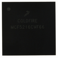
MCF5216CVF66 Freescale Semiconductor, MCF5216CVF66 Datasheet - Page 279

MCF5216CVF66
Manufacturer Part Number
MCF5216CVF66
Description
IC MPU 32BIT COLDF 256-MAPBGA
Manufacturer
Freescale Semiconductor
Series
MCF521xr
Datasheet
1.MCF5216CVM66J.pdf
(766 pages)
Specifications of MCF5216CVF66
Core Processor
Coldfire V2
Core Size
32-Bit
Speed
66MHz
Connectivity
CAN, EBI/EMI, I²C, SPI, UART/USART
Peripherals
DMA, LVD, POR, PWM, WDT
Number Of I /o
142
Program Memory Size
512KB (512K x 8)
Program Memory Type
FLASH
Ram Size
64K x 8
Voltage - Supply (vcc/vdd)
2.7 V ~ 3.6 V
Data Converters
A/D 8x12b
Oscillator Type
Internal
Operating Temperature
-40°C ~ 85°C
Package / Case
256-MAPBGA
Controller Family/series
ColdFire
Ram Memory Size
64KB
Embedded Interface Type
CAN, I2C, SPI, UART
No. Of Pwm Channels
8
Operating Temperature Range
-40°C To +85°C
No. Of Pins
256
Rohs Compliant
No
Package
256MA-BGA
Device Core
ColdFire
Family Name
MCF521x
Maximum Speed
66 MHz
Operating Supply Voltage
3.3 V
Data Bus Width
32 Bit
Number Of Programmable I/os
142
Interface Type
QSPI/UART/I2C/CAN
On-chip Adc
8-chx10-bit
Number Of Timers
8
Lead Free Status / RoHS Status
Contains lead / RoHS non-compliant
Eeprom Size
-
Available stocks
Company
Part Number
Manufacturer
Quantity
Price
Company:
Part Number:
MCF5216CVF66
Manufacturer:
FSC
Quantity:
1 670
Company:
Part Number:
MCF5216CVF66
Manufacturer:
Freescale Semiconductor
Quantity:
10 000
Part Number:
MCF5216CVF66
Manufacturer:
FREESCALE
Quantity:
20 000
Company:
Part Number:
MCF5216CVF66J
Manufacturer:
Freescale Semiconductor
Quantity:
10 000
- Current page: 279 of 766
- Download datasheet (9Mb)
Freescale Semiconductor
10–8
5–4
2–0
Bit
7
6
3
Name
IMRS Initiate mode register set (
CBM Command and bank MUX [2:0]. Because different SDRAM configurations cause the command and
PS
—
IP
—
bank select lines to correspond to different addresses, these resources are programmable. CBM
determines the addresses onto which these functions are multiplexed.
Note: It is important to set CBM according to the location of the command bit.
This encoding and the address multiplexing scheme handle common SDRAM organizations. Bank
select bits include a base bit and all address bits above for SDRAMs with multiple bank select bits.
Reserved, should be cleared.
SDRAMs. In initialization, IMRS should be set only after all DRAM controller registers are initialized
and
block programs the SDRAM’s mode register. Thus, the address of the access should be programmed
to place the correct mode information on the SDRAM address pins. Because the SDRAM does not
register this information, it doesn’t matter if the IMRS access is a read or a write or what, if any, data is
put onto the data bus. The DRAM controller clears IMRS after the
0 Take no action
1 Initiate
Port size. Indicates the port size of the associated block of SDRAM, which allows for dynamic sizing of
associated SDRAM accesses. PS functions the same in asynchronous operation.
00 32-bit port
01 8-bit port
1x 16-bit port
Initiate precharge all (
finished. Accesses via IP should be no wider than the port size programmed in PS.
0 Take no action.
1 A
Reserved, should be cleared.
executed after all DRAM controller registers are programmed. After IP is set, the next write to an
appropriate SDRAM address generates the
PALL
PALL
MCF5282 and MCF5216 ColdFire Microcontroller User’s Manual, Rev. 3
and
MRS
command is sent to the associated SDRAM block. During initialization, this command is
Table 15-5. DACRn Field Descriptions (continued)
REFRESH
command
PALL
commands have been issued. After IMRS is set, the next access to an SDRAM
MRS
) command. The DRAM controller clears IP after the
CBM
101
110
111
000
001
010
011
100
) command. Setting IMRS generates a
Command Bit
Description
PALL
17
18
19
20
21
22
23
24
command to the SDRAM block.
Bank Select Bits
18 and up
19 and up
20 and up
21 and up
22 and up
23 and up
24 and up
25 and up
MRS
Synchronous DRAM Controller Module
MRS
command finishes.
command to the associated
PALL
command is
15-7
Related parts for MCF5216CVF66
Image
Part Number
Description
Manufacturer
Datasheet
Request
R
Part Number:
Description:
Manufacturer:
Freescale Semiconductor, Inc
Datasheet:
Part Number:
Description:
Manufacturer:
Freescale Semiconductor, Inc
Datasheet:
Part Number:
Description:
Manufacturer:
Freescale Semiconductor, Inc
Datasheet:
Part Number:
Description:
Manufacturer:
Freescale Semiconductor, Inc
Datasheet:
Part Number:
Description:
Manufacturer:
Freescale Semiconductor, Inc
Datasheet:
Part Number:
Description:
Manufacturer:
Freescale Semiconductor, Inc
Datasheet:
Part Number:
Description:
Manufacturer:
Freescale Semiconductor, Inc
Datasheet:
Part Number:
Description:
Manufacturer:
Freescale Semiconductor, Inc
Datasheet:
Part Number:
Description:
Manufacturer:
Freescale Semiconductor, Inc
Datasheet:
Part Number:
Description:
Manufacturer:
Freescale Semiconductor, Inc
Datasheet:
Part Number:
Description:
Manufacturer:
Freescale Semiconductor, Inc
Datasheet:
Part Number:
Description:
Manufacturer:
Freescale Semiconductor, Inc
Datasheet:
Part Number:
Description:
Manufacturer:
Freescale Semiconductor, Inc
Datasheet:
Part Number:
Description:
Manufacturer:
Freescale Semiconductor, Inc
Datasheet:
Part Number:
Description:
Manufacturer:
Freescale Semiconductor, Inc
Datasheet:


