EM351-RTR Ember, EM351-RTR Datasheet - Page 150
EM351-RTR
Manufacturer Part Number
EM351-RTR
Description
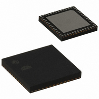
IC RF TXRX ZIGBEE 128KB 48QFN
Manufacturer
Ember
Specifications of EM351-RTR
Frequency
2.4GHz
Data Rate - Maximum
250kbps
Modulation Or Protocol
802.15.4 Zigbee
Power - Output
3dBm
Sensitivity
-100dBm
Voltage - Supply
2.1 V ~ 3.6 V
Current - Receiving
26mA
Current - Transmitting
31mA
Data Interface
PCB, Surface Mount
Memory Size
128kB Flash, 12kB RAM
Antenna Connector
PCB, Surface Mount
Operating Temperature
-40°C ~ 85°C
Package / Case
48-QFN
Lead Free Status / RoHS Status
Lead free / RoHS Compliant
Applications
-
Other names
636-1010-2
Available stocks
Company
Part Number
Manufacturer
Quantity
Price
Company:

Part Number:
EM351-RTR
Manufacturer:
SILICONLABOR
Quantity:
4 550


9.3.14.2
In this example, shown in Figure 9-32, the enable of Timer 2 is controlled with the output compare 1 of
Timer 1. Timer 2 counts on the divided internal clock only when OC1REF of Timer 1 is high. Both counter clock
frequencies are divided by 3 by the prescaler compared to CK_INT (f
Note: The counter 2 clock is not synchronized with counter 1, this mode only affects the Timer 2 counter
enable signal.
In the example in Figure 9-32, the Timer 2 counter and prescaler are not initialized before being started. So
they start counting from their current value. It is possible to start from a given value by resetting both timers
before starting Timer 1, then writing the desired value in the timer counters. The timers can easily be reset
by software using the TIM_UG bit in the TIMx_EGR registers.
The next example, illustrated in Figure 9-33, synchronizes Timer 1 and Timer 2. Timer 1 is the master and
starts from 0. Timer 2 is the slave and starts from 0xE7. The prescaler ratio is the same for both timers. Timer
2 stops when Timer 1 is disabled by writing 0 to the TIM_CEN bit in the TIM1_CR1 register:
Configure Timer 1 in master mode to send its Output Compare Reference (OC1REF) signal as trigger
output: Write TIM_MMS = 100 in the TIM1_CR2 register.
Configure the Timer 1 OC1REF waveform (TIM1_CCMR1 register).
Configure Timer 2 to get the input trigger from Timer 1: Write TIM_TS = 000 in the TIM2_SMCR register.
Configure Timer 2 in gated mode: Write TIM_SMS = 101 in the TIM2_SMCR register.
Enable Timer 2: Write 1 in the TIM_CEN bit in the TIM2_CR1 register.
Start Timer 1: Write 1 in the TIM_CEN bit in the TIM1_CR1 register.
Configure Timer 1 in master mode to send its Output Compare Reference (OC1REF) signal as trigger
output: Write TIM_MMS = 100 in the TIM1_CR2 register)
Configure the Timer 1 OC1REF waveform (TIM1_CCMR1 register).
Configure Timer 2 to get the input trigger from Timer 1: Write TIM_TS = 000 in the TIM2_SMCR register.
Configure Timer 2 in gated mode: Write TIM_SMS = 101 in the TIM2_SMCR register.
Reset Timer 1: Write 1 in the TIM_UG bit (TIM1_EGR register.
Reset Timer 2 by writing 1 in the TIM_UG bit (TIM2_EGR register).
Initialize Timer 2 to 0xE7: Write 0xE7 in the Timer 2 counter (TIM2_CNTL).
Enable Timer 2: Write 1 in the TIM_CEN bit in the TIM2_CR1 register.
Start Timer 1: Write 1 in the TIM_CEN bit in the TIM1_CR1 register.
Stop Timer 1: Write 0 in the TIM_CEN bit in the TIM1_CR1 register.
Using One Timer to Enable the Other Timer
Figure 9-32. Gating Timer 2 with OC1REF of Timer 1
Final
9-26
CK_CNT
= f
CK_INT
/3).
120-035X-000G
Related parts for EM351-RTR
Image
Part Number
Description
Manufacturer
Datasheet
Request
R

Part Number:
Description:
MODULE EM351 NO PA/LNA W/ANT TG
Manufacturer:
Ember
Datasheet:

Part Number:
Description:
MODULE EM351 NO PA/LNA W/RF CONN
Manufacturer:
Ember
Datasheet:

Part Number:
Description:
MODULE EM351 PA/LNA W/ANT TG
Manufacturer:
Ember
Datasheet:

Part Number:
Description:
MODULE EM351 PA/LNA W/RF CONN
Manufacturer:
Ember
Datasheet:

Part Number:
Description:
KIT DEV EMBER ZIGBEE W/PCWH
Manufacturer:
Custom Computer Services Inc (CCS)

Part Number:
Description:
PROGRAMMER USB FLASH EM250/260
Manufacturer:
Ember
Datasheet:

Part Number:
Description:
IC ZIGBEE SYSTEM-ON-CHIP 40-QFN
Manufacturer:
Ember
Datasheet:

Part Number:
Description:
IC ZIGBEE SYSTEM-ON-CHIP 48-QFN
Manufacturer:
Ember
Datasheet:
Part Number:
Description:
IC RF TXRX ZIGBEE 192KB 48QFN
Manufacturer:
Ember
Datasheet:

Part Number:
Description:
INSIGHT ADAPTER FOR EM2XX
Manufacturer:
Ember
Datasheet:

Part Number:
Description:
IAR EWARM LICENCE FOR EM35X
Manufacturer:
Ember
Datasheet:
Part Number:
Description:
PROGRAMMER USB FLASH EM250/260
Manufacturer:
Ember
Datasheet:
Part Number:
Description:
IC ZIGBEE SYSTEM-ON-CHIP 40-QFN
Manufacturer:
Ember
Datasheet:
Part Number:
Description:
IC ZIGBEE SYSTEM-ON-CHIP 48-QFN
Manufacturer:
Ember
Datasheet:
Part Number:
Description:
IC RF TXRX ZIGBEE 192KB 48QFN
Manufacturer:
Ember
Datasheet: