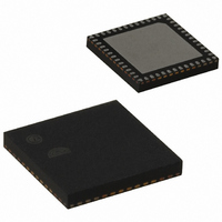
EM351-RTR Ember, EM351-RTR Datasheet - Page 57

EM351-RTR
Manufacturer Part Number
EM351-RTR
Description
IC RF TXRX ZIGBEE 128KB 48QFN
Manufacturer
Ember
Specifications of EM351-RTR
Frequency
2.4GHz
Data Rate - Maximum
250kbps
Modulation Or Protocol
802.15.4 Zigbee
Power - Output
3dBm
Sensitivity
-100dBm
Voltage - Supply
2.1 V ~ 3.6 V
Current - Receiving
26mA
Current - Transmitting
31mA
Data Interface
PCB, Surface Mount
Memory Size
128kB Flash, 12kB RAM
Antenna Connector
PCB, Surface Mount
Operating Temperature
-40°C ~ 85°C
Package / Case
48-QFN
Lead Free Status / RoHS Status
Lead free / RoHS Compliant
Applications
-
Other names
636-1010-2
Available stocks
Company
Part Number
Manufacturer
Quantity
Price
Company:
Part Number:
EM351-RTR
Manufacturer:
SILICONLABOR
Quantity:
4 550
- Current page: 57 of 245
- Download datasheet (12Mb)
7.4
7.5
Reset
Boot Configuration
and JTAG mode is forced when the EM35x resets, a designer must treat all four debug GPIOs as working in
unison even though the Serial Wire interface only uses one of the GPIO, PC4.
Note: An application must disable all debug SWJ debug functionality to reclaim any of the four GPIOs: PC0,
PC2, PC3, and PC4. Disabling SWJ debug functionality prevents external debug tools from operating, including
flash programming and high-level debug tools.
Disabling the SWJ debugger interface is accomplished by setting the GPIO_DEBUGDIS bit in the GPIO_DBGCFG
register. When this bit is set, all debugger-related pins (PC0, PC2, PC3, PC4) behave as standard GPIOs. If the
SWJ debugger interface is already active, the bit GPIO_DEBUGDIS cannot be set. When GPIO_DEBUGDIS is set,
the SWJ debugger interface can be reclaimed by activating the SWJ while the EM35x is held in reset. If the
SWJ debugger interface is forced active in this manner, the bit GPIO_FORCEDBG is set in the GPIO_DBGSTAT
register. The SWJ debugger interface is defined as active when the CDBGPWRUPREQ signal, a bit in the debug
port’s CRTL/STAT register in the SWJ, is set high by an external debug tool.
A full chip reset is one due to power on (low or high voltage), the nRESET pin, the watchdog, or the
SYSRESETREQ bit. A full chip reset affects the GPIO configuration as follows:
nBOOTMODE is a special alternate function of PA5 that is active only during a pin reset (nRESET) or a power-
on-reset of the always-powered domain (POR HV). If nBOOTMODE is asserted (pulled or driven low) when
coming out of reset, the processor starts executing an embedded serial-link-only boot loader instead of its
normal program.
While in reset and during the subsequent power-on-reset startup delay (512 OSCHF clocks), PA5 is
automatically configured as an input with a pull-up resistor. At the end of this time, the EM35x samples
nBOOTMODE: a high level selects normal boot mode, and a low level selects the embedded serial-link-only
boot loader (serial bootload mode). Figure 7-2 shows the timing parameters for invoking serial bootload mode
from a pin (nRESET) reset. Because OSCHF is running uncalibrated during the reset sequence, the time for 512
OSCHF clocks may vary as indicated.
The GPIO_PxCFGH/L configurations of all pins are configured as floating inputs.
The GPIO_EXTREGEN bit is set in the GPIO_DBGCFG register, which overrides the normal configuration for
PA7.
The GPIO_DEBUGDIS bit in the GPIO_DBGCFG register is cleared, allowing Serial Wire/JTAG access to
override the normal configuration of PC0, PC2, PC3, and PC4.
Final
7-4
EM351 / EM357
120-035X-000G
Related parts for EM351-RTR
Image
Part Number
Description
Manufacturer
Datasheet
Request
R

Part Number:
Description:
MODULE EM351 NO PA/LNA W/ANT TG
Manufacturer:
Ember
Datasheet:

Part Number:
Description:
MODULE EM351 NO PA/LNA W/RF CONN
Manufacturer:
Ember
Datasheet:

Part Number:
Description:
MODULE EM351 PA/LNA W/ANT TG
Manufacturer:
Ember
Datasheet:

Part Number:
Description:
MODULE EM351 PA/LNA W/RF CONN
Manufacturer:
Ember
Datasheet:

Part Number:
Description:
KIT DEV EMBER ZIGBEE W/PCWH
Manufacturer:
Custom Computer Services Inc (CCS)

Part Number:
Description:
PROGRAMMER USB FLASH EM250/260
Manufacturer:
Ember
Datasheet:

Part Number:
Description:
IC ZIGBEE SYSTEM-ON-CHIP 40-QFN
Manufacturer:
Ember
Datasheet:

Part Number:
Description:
IC ZIGBEE SYSTEM-ON-CHIP 48-QFN
Manufacturer:
Ember
Datasheet:

Part Number:
Description:
IC RF TXRX ZIGBEE 192KB 48QFN
Manufacturer:
Ember
Datasheet:

Part Number:
Description:
INSIGHT ADAPTER FOR EM2XX
Manufacturer:
Ember
Datasheet:

Part Number:
Description:
IAR EWARM LICENCE FOR EM35X
Manufacturer:
Ember
Datasheet:

Part Number:
Description:
PROGRAMMER USB FLASH EM250/260
Manufacturer:
Ember
Datasheet:

Part Number:
Description:
IC ZIGBEE SYSTEM-ON-CHIP 40-QFN
Manufacturer:
Ember
Datasheet:

Part Number:
Description:
IC ZIGBEE SYSTEM-ON-CHIP 48-QFN
Manufacturer:
Ember
Datasheet:

Part Number:
Description:
IC RF TXRX ZIGBEE 192KB 48QFN
Manufacturer:
Ember
Datasheet:


