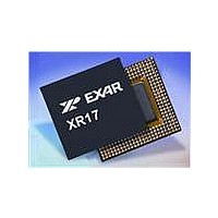
XR17V354IB176-F Exar Corporation, XR17V354IB176-F Datasheet - Page 25

XR17V354IB176-F
Manufacturer Part Number
XR17V354IB176-F
Description
IC UART PCIE 256B DUAL 176FPBGA
Manufacturer
Exar Corporation
Datasheet
1.XR17V354IB176-F.pdf
(66 pages)
Specifications of XR17V354IB176-F
Number Of Channels
4, QUART
Package / Case
176-LFBGA
Features
*
Fifo's
256 Byte
Protocol
RS485
Voltage - Supply
3.3V
With Auto Flow Control
Yes
With Irda Encoder/decoder
Yes
With False Start Bit Detection
Yes
With Modem Control
Yes
Mounting Type
Surface Mount
Data Rate
25 Mbps
Supply Current
120 mA
Maximum Operating Temperature
+ 85 C
Minimum Operating Temperature
- 40 C
Mounting Style
SMD/SMT
Operating Supply Voltage
3.3 V
No. Of Channels
4
Uart Features
Tx/Rx FIFO Counters
Supply Voltage Range
3V To 3.6V
Operating Temperature Range
-40°C To +85°C
Digital Ic Case Style
BGA
No. Of Pins
176
Rohs Compliant
Yes
Lead Free Status / RoHS Status
Lead free / RoHS Compliant
Lead Free Status / RoHS Status
Lead free / RoHS Compliant, Lead free / RoHS Compliant
Available stocks
Company
Part Number
Manufacturer
Quantity
Price
Company:
Part Number:
XR17V354IB176-F
Manufacturer:
EXAR
Quantity:
500
Company:
Part Number:
XR17V354IB176-F
Manufacturer:
Exar Corporation
Quantity:
10 000
Part Number:
XR17V354IB176-F
Manufacturer:
EXAR/艾科嘉
Quantity:
20 000
REV. 1.0.1
The V354 provides 16 multi-purpose inputs/outputs MPIO[15:0] for general use. Each pin can be programmed
to be an input or output function. The input logic state can be set for normal or inverted level, and optionally set
to generate an interrupt. The outputs can be set to be normal HIGH or LOW state, 3-state, or open drain. Their
functions and definitions are programmed through 6 registers: MPIOINT, MPIOLVL, MPIO3T, MPIOINV,
MPIOSEL, and MPIOOD. If all 16 pins are set for inputs, all 16 interrupts would be ORed together. The ORed
interrupt is reported in the channel 0 UART interrupt status, see Interrupt Status Register. The pins may also be
programmed to be outputs and to the 3-state condition for signal sharing. The MPIO[0] pin can be programmed
to show the Timer output. When it is programmed to be the Timer output, all the above 5 registers lose control
over the MPIO[0] pin. For details on Timer output, please see
Counter [TIMERMSB, TIMELSB, TIMER, TIMECNTL] (default 0xXX-XX-00-00)” on page
REGB[18](Read/Write
REGB[19](Read-Only)
REGB[20] (Write-Only)
REGB[21] (Write-Only)
REGB[22] (Write-Only)
REGB[23] (Read-Only)
1.4.7
1.4.8
1.4.9
REGB Register
Multi-Purpose Inputs and Outputs
MPIO REGISTERS
Logic 0 (default) - Global interrupt enable. Interrupts to PCI host are enabled.
Control the EECS, chips select, output to the EEPROM device.
EEDO data output. Read data from the EEPROM device.
Logic 1 - Global interrupt disable. Interrupts to PCI host are disabled.
Logic 0 - EEPROM load is valid.
Logic 1 - EEPROM load error caused by one of the following conditions: EEPROM not
attached, final bit not found, parity error detected.
Control the EECK, clock, output on the EEPROM interface.
EEDI data input. Write data to the EEPROM device.
25
HIGH PERFORMANCE QUAD PCI-EXPRESS UART
“Section 1.4.2, General Purpose 16-bit Timer/
19.
XR17V354


