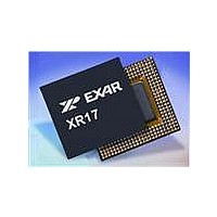
XR17V354IB176-F Exar Corporation, XR17V354IB176-F Datasheet - Page 31

XR17V354IB176-F
Manufacturer Part Number
XR17V354IB176-F
Description
IC UART PCIE 256B DUAL 176FPBGA
Manufacturer
Exar Corporation
Datasheet
1.XR17V354IB176-F.pdf
(66 pages)
Specifications of XR17V354IB176-F
Number Of Channels
4, QUART
Package / Case
176-LFBGA
Features
*
Fifo's
256 Byte
Protocol
RS485
Voltage - Supply
3.3V
With Auto Flow Control
Yes
With Irda Encoder/decoder
Yes
With False Start Bit Detection
Yes
With Modem Control
Yes
Mounting Type
Surface Mount
Data Rate
25 Mbps
Supply Current
120 mA
Maximum Operating Temperature
+ 85 C
Minimum Operating Temperature
- 40 C
Mounting Style
SMD/SMT
Operating Supply Voltage
3.3 V
No. Of Channels
4
Uart Features
Tx/Rx FIFO Counters
Supply Voltage Range
3V To 3.6V
Operating Temperature Range
-40°C To +85°C
Digital Ic Case Style
BGA
No. Of Pins
176
Rohs Compliant
Yes
Lead Free Status / RoHS Status
Lead free / RoHS Compliant
Lead Free Status / RoHS Status
Lead free / RoHS Compliant, Lead free / RoHS Compliant
Available stocks
Company
Part Number
Manufacturer
Quantity
Price
Company:
Part Number:
XR17V354IB176-F
Manufacturer:
EXAR
Quantity:
500
Company:
Part Number:
XR17V354IB176-F
Manufacturer:
Exar Corporation
Quantity:
10 000
Part Number:
XR17V354IB176-F
Manufacturer:
EXAR/艾科嘉
Quantity:
20 000
REV. 1.0.1
The THR and RHR register address for channel 0 to channel 3 is shown in
for each channel 0 to 3 are located sequentially at address 0x0000, 0x0200, 0x0400 and 0x0600. Transmit
data byte is loaded to the THR when writing to that address and receive data is unloaded from the RHR
register when reading that address. Both THR and RHR registers are 16C550 compatible in 8-bit format, so
each bus operation can only write or read in bytes.
2.2
Data Bit-31
PCI Bus
B7 B6 B5 B4 B3 B2 B1 B0
FIFO DATA LOADING AND UNLOADING THROUGH THE UART CHANNEL REGISTERS, THR
AND RHR IN 8-BIT FORMAT
Transmit Data Byte n+3
T
ABLE
10: T
CH3 0xC000 Read THR
CH3 0xC000 Write RHR
CH0 0x0000 Read THR
CH0 0x0000 Write RHR
CH1 0x4000 Read THR
CH1 0x4000 Write RHR
CH2 0x8000 Read THR
CH2 0x8000 Write RHR
RANSMIT AND
Channel 0 to 3 Transmit Data in 32-bit alignment through the Configuration Register Address
THR and RHR Address Locations For CH0 to CH3 (16C550 Compatible)
B7 B6 B5 B4 B3 B2 B1 B0
Transmit Data Byte n+2
R
ECEIVE
Bit-7
Bit-7
Bit-7
Bit-7
Bit-7
Bit-7
Bit-7
Bit-7
0x0100, 0x0500, 0x0900 and 0x0D00
D
ATA
Bit-6
Bit-6
Bit-6
Bit-6
Bit-6
Bit-6
Bit-6
Bit-6
R
EGISTER IN
31
Bit-5
Bit-5
Bit-5
Bit-5
Bit-5
Bit-5
Bit-5
Bit-5
HIGH PERFORMANCE QUAD PCI-EXPRESS UART
B7 B6 B5 B4 B3 B2 B1 B0
Bit-4
Bit-4
Bit-4
Bit-4
Bit-4
Bit-4
Bit-4
Bit-4
Transmit Data Byte n+1
B
YTE FORMAT
Bit-3
Bit-3
Bit-3
Bit-3
Bit-3
Bit-3
Bit-3
Bit-3
Bit-2
Bit-2
Bit-2
Bit-2
Bit-2
Bit-2
Bit-2
Bit-2
Table 10
, 16C550
Bit-1
Bit-1
Bit-1
Bit-1
Bit-1
Bit-1
Bit-1
Bit-1
B7 B6 B5 B4 B3 B2 B1 B0
below. The THR and RHR
Bit-0
Bit-0
Bit-0
Bit-0
Bit-0
Bit-0
Bit-0
Bit-0
Transmit Data Byte n+0
COMPATIBLE
XR17V354
Data Bit-0
PCI Bus


