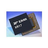
XR17V354IB176-F Exar Corporation, XR17V354IB176-F Datasheet - Page 51

XR17V354IB176-F
Manufacturer Part Number
XR17V354IB176-F
Description
IC UART PCIE 256B DUAL 176FPBGA
Manufacturer
Exar Corporation
Datasheet
1.XR17V354IB176-F.pdf
(66 pages)
Specifications of XR17V354IB176-F
Number Of Channels
4, QUART
Package / Case
176-LFBGA
Features
*
Fifo's
256 Byte
Protocol
RS485
Voltage - Supply
3.3V
With Auto Flow Control
Yes
With Irda Encoder/decoder
Yes
With False Start Bit Detection
Yes
With Modem Control
Yes
Mounting Type
Surface Mount
Data Rate
25 Mbps
Supply Current
120 mA
Maximum Operating Temperature
+ 85 C
Minimum Operating Temperature
- 40 C
Mounting Style
SMD/SMT
Operating Supply Voltage
3.3 V
No. Of Channels
4
Uart Features
Tx/Rx FIFO Counters
Supply Voltage Range
3V To 3.6V
Operating Temperature Range
-40°C To +85°C
Digital Ic Case Style
BGA
No. Of Pins
176
Rohs Compliant
Yes
Lead Free Status / RoHS Status
Lead free / RoHS Compliant
Lead Free Status / RoHS Status
Lead free / RoHS Compliant, Lead free / RoHS Compliant
Available stocks
Company
Part Number
Manufacturer
Quantity
Price
Company:
Part Number:
XR17V354IB176-F
Manufacturer:
EXAR
Quantity:
500
Company:
Part Number:
XR17V354IB176-F
Manufacturer:
Exar Corporation
Quantity:
10 000
Part Number:
XR17V354IB176-F
Manufacturer:
EXAR/艾科嘉
Quantity:
20 000
REV. 1.0.1
The Line Control Register is used to specify the asynchronous data communication format. The word or
character length, the number of stop bits, and the parity are selected by writing the appropriate bits in this
register.
LCR[7]: Baud Rate Divisors Enable
Baud rate generator divisor (DLL, DLM, DLD) enable.
•
•
LCR[6]: Transmit Break Enable
When enabled the Break control bit causes a break condition to be transmitted (the TX output is forced to a
“space", LOW, state). This condition remains until disabled by setting LCR bit [6] to a logic 0.
•
•
LCR[5]: TX and RX Parity Select
If the parity bit is enabled, LCR bit [5] selects the forced parity format.
•
•
•
4.7
Logic 0 = Data registers are selected (default).
Logic 1 = Divisor latch registers (DLL, DLM and DLD) are selected.
Logic 0 = No TX break condition. (default)
Logic 1 = Forces the transmitter output (TX) to a “space”, LOW, for alerting the remote receiver of a line
break condition.
LCR bit [5] = logic 0, parity is not forced (default).
LCR bit [5] = logic 1 and LCR bit [4] = logic 0, parity bit is forced to a logical 1for the transmit and receive
data.
LCR bit [5] = logic 1 and LCR bit [4] = logic 1, parity bit is forced to a logical 0 for the transmit and receive
data.
T
Table-C
Table-D
RIGGER
T
ABLE
Line Control Register (LCR) - Read/Write
BIT [7]
FCTR
1
1
T
ABLE
BIT [6]
FCTR
16: T
0
1
RANSMIT AND
BIT [7]
FCR
X
0
0
1
1
BIT [6]
FCR
X
0
1
0
1
R
ECEIVE
BIT [5]
FCR
X
0
0
1
1
FIFO T
BIT [4]
51
FCR
HIGH PERFORMANCE QUAD PCI-EXPRESS UART
X
0
1
0
1
RIGGER
T
Programmable
RIGGER
via RXTRG
R
T
register
ABLE AND
ECEIVE
16
56
60
8
L
EVEL
L
Programmable
EVEL
via TXTRG
T
T
register
RANSMIT
RIGGER
L
EVEL
16
32
56
8
S
ELECTION
16C654
16L2752, 16L2750,
16C2852, 16C850,
16C854, 16C864
C
XR17V354
OMPATIBILITY


