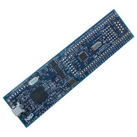
OM13012,598 NXP Semiconductors, OM13012,598 Datasheet - Page 10

OM13012,598
Manufacturer Part Number
OM13012,598
Description
BOARD EVAL LPC11C2X
Manufacturer
NXP Semiconductors
Datasheet
1.LPC11C14FBD48301.pdf
(61 pages)
Specifications of OM13012,598
Featured Product
32-bit ARM Cortex-M0 Microcontrollers
Processor To Be Evaluated
LPC11C2x
Data Bus Width
32 bit
Core
ARM Cortex-M0
Maximum Operating Temperature
+ 85 C
Minimum Operating Temperature
- 40 C
Operating Supply Voltage
3.3 V
Lead Free Status / RoHS Status
Lead free / RoHS Compliant
Lead Free Status / RoHS Status
Lead free / RoHS Compliant, Lead free / RoHS Compliant
Other names
568-6645
OM13012
OM13012
NXP Semiconductors
Table 3.
[1]
[2]
[3]
[4]
[5]
[6]
[7]
Table 4.
LPC11CX2_CX4
Product data sheet
Symbol
PIO3_0/DTR
PIO3_1/DSR
PIO3_2/DCD
PIO3_3/RI
CAN_RXD
CAN_TXD
V
XTALIN
XTALOUT
V
Symbol
PIO0_0 to PIO0_11
RESET/PIO0_0
DD
SS
Pin state at reset for default function: I = Input; O = Output; PU = internal pull-up enabled; IA = inactive, no pull-up/down enabled.
See
reset the chip and wake up from Deep power-down mode. An external pull-up resistor is required on this pin for the Deep power-down
mode.
5 V tolerant pad providing digital I/O functions with configurable pull-up/pull-down resistors and configurable hysteresis (see
I
5 V tolerant pad providing digital I/O functions with configurable pull-up/pull-down resistors, configurable hysteresis, and analog input.
When configured as a ADC input, digital section of the pad is disabled and the pin is not 5 V tolerant (see
5 V tolerant digital I/O pad without pull-up/pull-down resistors.
When the system oscillator is not used, connect XTALIN and XTALOUT as follows: XTALIN can be left floating or can be grounded
(grounding is preferred to reduce susceptibility to noise). XTALOUT should be left floating.
2
C-bus pads compliant with the I
Figure 26
LPC11C12/C14 pin description table
LPC11C22/C24 pin description table
for reset pad configuration. RESET functionality is not available in Deep power-down mode. Use the WAKEUP pin to
Pin
36
37
43
48
19
20
8; 44
6
7
5; 41
Pin
3
[7]
[7]
[2]
[3]
[3]
[3]
[3]
[6]
[6]
Start
logic
inputs
no
no
no
no
no
no
-
-
-
-
Start
logic
inputs
yes
2
C-bus specification for I
Type
I/O
O
I/O
I
I/O
I
I/O
I
I
O
I
I
O
I
Type
I
I/O
All information provided in this document is subject to legal disclaimers.
Reset
state
[1]
I; PU
-
I; PU
-
I; PU
I; PU
-
I; IA
I; IA
-
-
-
-
Reset
state
[1]
I; PU
-
Rev. 2 — 3 December 2010
Supply voltage to the internal regulator, the external rail, and the
Ground.
Description
PIO3_0 — General purpose digital input/output pin.
DTR — Data Terminal Ready output for UART.
PIO3_1 — General purpose digital input/output pin.
DSR — Data Set Ready input for UART.
PIO3_2 — General purpose digital input/output pin.
DCD — Data Carrier Detect input for UART.
PIO3_3 — General purpose digital input/output pin.
RI — Ring Indicator input for UART.
CAN_RXD — C_CAN receive data input.
CAN_TXD — C_CAN transmit data output.
ADC. Also used as the ADC reference voltage.
Input to the oscillator circuit and internal clock generator circuits.
Input voltage must not exceed 1.8 V.
Output from the oscillator amplifier.
Description
Port 0 — Port 0 is a 12-bit I/O port with individual direction and
function controls for each bit. The operation of port 0 pins depends
on the function selected through the IOCONFIG register block.
RESET — External reset input with 20 ns glitch filter. A LOW-going
pulse as short as 50 ns on this pin resets the device, causing I/O
ports and peripherals to take on their default states, and processor
execution to begin at address 0.
PIO0_0 — General purpose digital input/output pin with 10 ns glitch
filter.
2
C standard mode and I
2
C Fast-mode Plus.
32-bit ARM Cortex-M0 microcontroller
LPC11Cx2/Cx4
Figure
© NXP B.V. 2010. All rights reserved.
25).
Figure
10 of 61
25).


