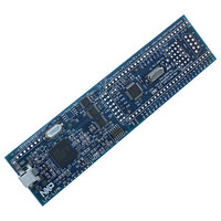
OM13012,598 NXP Semiconductors, OM13012,598 Datasheet - Page 47

OM13012,598
Manufacturer Part Number
OM13012,598
Description
BOARD EVAL LPC11C2X
Manufacturer
NXP Semiconductors
Datasheet
1.LPC11C14FBD48301.pdf
(61 pages)
Specifications of OM13012,598
Featured Product
32-bit ARM Cortex-M0 Microcontrollers
Processor To Be Evaluated
LPC11C2x
Data Bus Width
32 bit
Core
ARM Cortex-M0
Maximum Operating Temperature
+ 85 C
Minimum Operating Temperature
- 40 C
Operating Supply Voltage
3.3 V
Lead Free Status / RoHS Status
Lead free / RoHS Compliant
Lead Free Status / RoHS Status
Lead free / RoHS Compliant, Lead free / RoHS Compliant
Other names
568-6645
OM13012
OM13012
NXP Semiconductors
Table 18.
LPC11CX2_CX4
Product data sheet
Symbol
SPI master (in SPI mode)
T
t
t
t
t
SPI slave (in SPI mode)
T
DS
DH
v(Q)
h(Q)
Fig 20. I
cy(clk)
cy(PCLK)
SDA
SCL
2
C-bus pins clock timing
Dynamic characteristics of SPI pins in SPI mode
Parameter
clock cycle time
data set-up time
data hold time
data output valid time in SPI mode
data output hold time in SPI mode
PCLK cycle time
70 %
30 %
S
10.6 SPI interfaces
t
f
t
f
70 %
[6]
[7]
[8]
[9]
[10] A Fast-mode I
30 %
The maximum t
output stage t
SDA and the SCL pins and the SDA/SCL bus lines without exceeding the maximum specified t
In Fast-mode Plus, fall time is specified the same for both output stage and bus timing. If series resistors
are used, designers should allow for this when considering bus timing.
The maximum t
the maximum of t
the device does not stretch the LOW period (t
data must be valid by the set-up time before it releases the clock.
tSU;DAT is the data set-up time that is measured with respect to the rising edge of SCL; applies to data in
transmission and the acknowledge.
250 ns must then be met. This will automatically be the case if the device does not stretch the LOW period
of the SCL signal. If such a device does stretch the LOW period of the SCL signal, it must output the next
data bit to the SDA line t
specification) before the SCL line is released. Also the acknowledge timing must meet this set-up time.
1 / f
SCL
Conditions
when only receiving
when only transmitting
in SPI mode
in SPI mode
t
2.4 V V
2.0 V V
1.8 V V
HD;DAT
70 %
30 %
f
70 %
2
30 %
All information provided in this document is subject to legal disclaimers.
is specified at 250 ns. This allows series protection resistors to be connected in between the
C-bus device can be used in a Standard-mode I
HD;DAT
f
for the SDA and SCL bus lines is specified at 300 ns. The maximum fall time for the SDA
VD;DAT
t
SU;DAT
DD
DD
DD
could be 3.45 s and 0.9 s for Standard-mode and Fast-mode but must be less than
Rev. 2 — 3 December 2010
3.6 V
< 2.4 V
< 2.0 V
or t
r(max)
VD;ACK
+ t
70 %
SU;DAT
30 %
[1]
[1]
[2]
[2]
[2]
[2]
[2]
[2]
by a transition time (see UM10204). This maximum must only be met if
t
LOW
= 1000 + 250 = 1250 ns (according to the Standard-mode I
Min
40
27.8
15
20
24
0
-
0
20
LOW
) of the SCL signal. If the clock stretches the SCL, the
t
HIGH
32-bit ARM Cortex-M0 microcontroller
70 %
30 %
t
2
VD;DAT
C-bus system but the requirement t
Typ
-
-
-
-
-
-
-
LPC11Cx2/Cx4
Max
-
-
-
-
10
-
-
© NXP B.V. 2010. All rights reserved.
002aaf425
f
.
2
SU;DAT
47 of 61
C-bus
ns
ns
ns
ns
ns
ns
ns
ns
Unit
ns
=


