OM13012,598 NXP Semiconductors, OM13012,598 Datasheet - Page 9
OM13012,598
Manufacturer Part Number
OM13012,598
Description
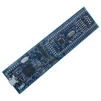
BOARD EVAL LPC11C2X
Manufacturer
NXP Semiconductors
Datasheet
1.LPC11C14FBD48301.pdf
(61 pages)
Specifications of OM13012,598
Featured Product
32-bit ARM Cortex-M0 Microcontrollers
Processor To Be Evaluated
LPC11C2x
Data Bus Width
32 bit
Core
ARM Cortex-M0
Maximum Operating Temperature
+ 85 C
Minimum Operating Temperature
- 40 C
Operating Supply Voltage
3.3 V
Lead Free Status / RoHS Status
Lead free / RoHS Compliant
Lead Free Status / RoHS Status
Lead free / RoHS Compliant, Lead free / RoHS Compliant
Other names
568-6645
OM13012
OM13012


NXP Semiconductors
Table 3.
LPC11CX2_CX4
Product data sheet
Symbol
PIO1_7/TXD/
CT32B0_MAT1
PIO1_8/
CT16B1_CAP0
PIO1_9/
CT16B1_MAT0
PIO1_10/AD6/
CT16B1_MAT1
PIO1_11/AD7
PIO2_0 to PIO2_11
PIO2_0/DTR/
SSEL1
PIO2_1/DSR/SCK1 13
PIO2_2/DCD/
MISO1
PIO2_3/RI/MOSI1
PIO2_4
PIO2_5
PIO2_6
PIO2_7
PIO2_8
PIO2_9
PIO2_10
PIO2_11/SCK0
PIO3_0 to PIO3_3
LPC11C12/C14 pin description table
Pin
47
9
17
30
42
2
26
38
18
21
1
11
12
24
25
31
[3]
[3]
[3]
[3]
[3]
[3]
[5]
[5]
[3]
[3]
[3]
[3]
[3]
[3]
[3]
[3]
[3]
Start
logic
inputs
no
no
no
no
no
no
no
no
no
no
no
no
no
no
no
no
no
Type
I/O
O
O
I/O
I
I/O
O
I/O
I
O
I/O
I
I/O
I/O
I/O
I/O
I
I/O
I/O
I
I/O
I/O
I
I/O
I/O
I/O
I/O
I/O
I/O
I/O
I/O
I/O
I/O
All information provided in this document is subject to legal disclaimers.
Reset
state
[1]
I; PU
-
-
I; PU
-
I; PU
-
I; PU
-
-
I; PU
-
I; PU
-
-
I; PU
-
-
I; PU
-
-
I; PU
-
-
I; PU
I; PU
I; PU
I; PU
I; PU
I; PU
I; PU
I; PU
-
Rev. 2 — 3 December 2010
Description
PIO1_7 — General purpose digital input/output pin.
TXD — Transmitter output for UART.
CT32B0_MAT1 — Match output 1 for 32-bit timer 0.
PIO1_8 — General purpose digital input/output pin.
CT16B1_CAP0 — Capture input 0 for 16-bit timer 1.
PIO1_9 — General purpose digital input/output pin.
CT16B1_MAT0 — Match output 0 for 16-bit timer 1.
PIO1_10 — General purpose digital input/output pin.
AD6 — A/D converter, input 6.
CT16B1_MAT1 — Match output 1 for 16-bit timer 1.
PIO1_11 — General purpose digital input/output pin.
AD7 — A/D converter, input 7.
Port 2 — Port 2 is a 12-bit I/O port with individual direction and
function controls for each bit. The operation of port 2 pins depends
on the function selected through the IOCONFIG register block.
PIO2_0 — General purpose digital input/output pin.
DTR — Data Terminal Ready output for UART.
SSEL1 — Slave Select for SPI1.
PIO2_1 — General purpose digital input/output pin.
DSR — Data Set Ready input for UART.
SCK1 — Serial clock for SPI1.
PIO2_2 — General purpose digital input/output pin.
DCD — Data Carrier Detect input for UART.
MISO1 — Master In Slave Out for SPI1.
PIO2_3 — General purpose digital input/output pin.
RI — Ring Indicator input for UART.
MOSI1 — Master Out Slave In for SPI1.
PIO2_4 — General purpose digital input/output pin.
PIO2_5 — General purpose digital input/output pin.
PIO2_6 — General purpose digital input/output pin.
PIO2_7 — General purpose digital input/output pin.
PIO2_8 — General purpose digital input/output pin.
PIO2_9 — General purpose digital input/output pin.
PIO2_10 — General purpose digital input/output pin.
PIO2_11 — General purpose digital input/output pin.
SCK0 — Serial clock for SPI0.
Port 3 — Port 3 is a 12-bit I/O port with individual direction and
function controls for each bit. The operation of port 3 pins depends
on the function selected through the IOCONFIG register block. Pins
PIO3_4 to PIO3_11 are not available.
32-bit ARM Cortex-M0 microcontroller
LPC11Cx2/Cx4
© NXP B.V. 2010. All rights reserved.
9 of 61
Related parts for OM13012,598
Image
Part Number
Description
Manufacturer
Datasheet
Request
R

Part Number:
Description:
NXP Semiconductors designed the LPC2420/2460 microcontroller around a 16-bit/32-bitARM7TDMI-S CPU core with real-time debug interfaces that include both JTAG andembedded trace
Manufacturer:
NXP Semiconductors
Datasheet:

Part Number:
Description:
NXP Semiconductors designed the LPC2458 microcontroller around a 16-bit/32-bitARM7TDMI-S CPU core with real-time debug interfaces that include both JTAG andembedded trace
Manufacturer:
NXP Semiconductors
Datasheet:
Part Number:
Description:
NXP Semiconductors designed the LPC2468 microcontroller around a 16-bit/32-bitARM7TDMI-S CPU core with real-time debug interfaces that include both JTAG andembedded trace
Manufacturer:
NXP Semiconductors
Datasheet:
Part Number:
Description:
NXP Semiconductors designed the LPC2470 microcontroller, powered by theARM7TDMI-S core, to be a highly integrated microcontroller for a wide range ofapplications that require advanced communications and high quality graphic displays
Manufacturer:
NXP Semiconductors
Datasheet:
Part Number:
Description:
NXP Semiconductors designed the LPC2478 microcontroller, powered by theARM7TDMI-S core, to be a highly integrated microcontroller for a wide range ofapplications that require advanced communications and high quality graphic displays
Manufacturer:
NXP Semiconductors
Datasheet:
Part Number:
Description:
The Philips Semiconductors XA (eXtended Architecture) family of 16-bit single-chip microcontrollers is powerful enough to easily handle the requirements of high performance embedded applications, yet inexpensive enough to compete in the market for hi
Manufacturer:
NXP Semiconductors
Datasheet:
Part Number:
Description:
The XA-S3 device is a member of Philips Semiconductors? XA(eXtended Architecture) family of high performance 16-bitsingle-chip microcontrollers
Manufacturer:
NXP Semiconductors
Datasheet:

Part Number:
Description:
The NXP BlueStreak LH75401/LH75411 family consists of two low-cost 16/32-bit System-on-Chip (SoC) devices
Manufacturer:
NXP Semiconductors
Datasheet:
Part Number:
Description:
The NXP LPC3130/3131 combine an 180 MHz ARM926EJ-S CPU core, high-speed USB2
Manufacturer:
NXP Semiconductors
Datasheet:
Part Number:
Description:
The NXP LPC3141 combine a 270 MHz ARM926EJ-S CPU core, High-speed USB 2
Manufacturer:
NXP Semiconductors
Part Number:
Description:
The NXP LPC3143 combine a 270 MHz ARM926EJ-S CPU core, High-speed USB 2
Manufacturer:
NXP Semiconductors

Part Number:
Description:
The NXP LPC3152 combines an 180 MHz ARM926EJ-S CPU core, High-speed USB 2
Manufacturer:
NXP Semiconductors
Part Number:
Description:
The NXP LPC3154 combines an 180 MHz ARM926EJ-S CPU core, High-speed USB 2
Manufacturer:
NXP Semiconductors

Part Number:
Description:
Standard level N-channel enhancement mode Field-Effect Transistor (FET) in a plastic package using NXP High-Performance Automotive (HPA) TrenchMOS technology
Manufacturer:
NXP Semiconductors
Datasheet: