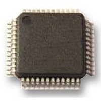
DP83848VYB National Semiconductor, DP83848VYB Datasheet - Page 28

DP83848VYB
Manufacturer Part Number
DP83848VYB
Description
TRANSCEIVER, ENET PHY, 10/100, 48LQFP
Manufacturer
National Semiconductor
Datasheet
1.DP83848VYB.pdf
(76 pages)
Specifications of DP83848VYB
Data Rate
100Mbps
No. Of Ports
1
Ethernet Type
IEEE 802.3u
Supply Current
92mA
Supply Voltage Range
3V To 3.6V
Operating Temperature Range
-40°C To +105°C
Digital Ic Case Style
LQFP
No.
RoHS Compliant
Interface Type
MII Serial, RMII
Rohs Compliant
Yes
Lead Free Status / Rohs Status
Not Compliant
Available stocks
Company
Part Number
Manufacturer
Quantity
Price
Company:
Part Number:
DP83848VYB/NOPB
Manufacturer:
NS
Quantity:
570
Company:
Part Number:
DP83848VYB/NOPB
Manufacturer:
Texas Instruments
Quantity:
10 000
www.national.com
5.0 Design Guidelines
5.1 TPI NETWORK CIRCUIT
Figure 10 shows the recommended circuit for a 10/100 Mb/s
twisted pair interface. To the right is a partial list of recom-
mended transformers. It is important that the user realize that
variations with PCB and component characteristics requires
5.2 ESD PROTECTION
Typically, ESD precautions are predominantly in effect when
handling the devices or board before being installed in a sys-
tem. In those cases, strict handling procedures need be im-
plemented during the manufacturing process to greatly
reduce the occurrences of catastrophic ESD events. After the
system is assembled, internal components are less sensitive
from ESD events.
See section 8.0 AC and DC Specifications for ESD rating.
5.3 CLOCK IN (X1) REQUIREMENTS
The DP83848VYB supports an external CMOS level oscilla-
tor source or a crystal resonator device.
Oscillator
If an external clock source is used, X1 should be tied to the
clock source and X2 should be left floating.
Specifications for CMOS oscillators: 25 MHz in MII Mode and
50 MHz in RMII Mode are listed in Table 7 and Table 8.
FIGURE 10. 10/100 Mb/s Twisted Pair Interface
28
that the application be tested to ensure that the circuit meets
the requirements of the intended application.
Crystal
A 25 MHz, parallel, 20 pF load crystal resonator should be
used if a crystal source is desired. Figure 12 shows a typical
connection for a crystal resonator circuit. The load capacitor
values will vary with the crystal vendors; check with the ven-
dor for the recommended loads.
The oscillator circuit is designed to drive a parallel resonance
AT cut crystal with a minimum drive level of 100mW and a
maximum of 500 µW. If a crystal is specified for a lower drive
level, a current limiting resistor should be placed in series be-
tween X2 and the crystal.
As a starting point for evaluating an oscillator circuit, if the
requirements for the crystal are not known, C
should be set at 33 pF, and R
Specification for 25 MHz crystal are listed in Table 9.
Pulse H1102
Pulse H2019
Pulse J0011D21
Pulse J0011D21B
1
should be set at 0Ω.
30011711
L1
and C
L2


